
Main navigation

  • Home
  • Discover
  • Learning Center
  • What’s New

Second main navigation

  • Altium Community
  • Support
  • Documentation
×

Results

  • Updates
  • Blog 571
  • Video 540
  • Webinar 86
  • Playlist 53
Filters:
Tag (field_common_tag)
Embedded thumbnail for Altium Develop: Returning to Our Roots
How-To's • Nov 5, 2025
Altium Develop: Returning to Our Roots

Lawrence Romine unveils Altium’s groundbreaking approach to product development with Altium Develop. This innovative solution realigns the company with its core mission - empowering individual engineers and small teams. Explore the strategic vision behind creating a product that seamlessly balances accessibility, robust functionality, and intuitive design.

Start Watching
Blog • Nov 4, 2025
6 Areas Your PCB Design Reviews Should Focus On

Learn the six essential topics every electronics team should address in design reviews to improve quality, avoid surprises and bring products to market faster.

Read More
Embedded thumbnail for Altium Training - Navigating Schematics: Schematic Preference Settings for Navigation
Altium Training • Nov 3, 2025
Altium Training - Navigating Schematics: Schematic Preference Settings for Navigation

Unlock smarter design navigation in Altium! Learn how to customize navigation preferences to boost your design insight and visualize connectivity like never before. In this video, we’ll explore Design Insight settings, interactive connectivity hover features, and quick thumbnail navigation between schematic sheets. All designed to make your workflow faster, clearer, and more intuitive.

Start Watching
Blog • Oct 30, 2025
What Is BOM Management? A Practical Guide to Avoiding Costly Part Mismatches

From design to production, effective Bill of Materials (BOM) management is critical to ensuring smooth collaboration between engineering, procurement, and manufacturing teams. In this practical guide, we break down proven strategies for structuring, maintaining, and synchronizing your BOM to prevent costly mistakes and accelerate time-to-market.

Read More
Blog • Oct 29, 2025
Requirements Portal Introductory Tutorials

This series of guided demos shows how the Altium Requirements Portal transforms scattered requirement spreadsheets and emails into traceable, version-controlled data that stays aligned with your PCB design efforts.

Read More
Embedded thumbnail for PCB Design Tools for Every Team Size: Altium's New Approach
How-To's • Oct 28, 2025
PCB Design Tools for Every Team Size: Altium's New Approach

Explore how Altium is transforming PCB design with software solutions built for teams of every size. In this exclusive PCB West 2025 interview, Justin Sears highlights the key distinctions between Altium Develop and Altium Agile helping you identify the ideal platform for your design needs.

Start Watching
Blog • Oct 27, 2025
Bridging the Gap: When to Use Rigid-Flex Instead of Flex & Connector

Discover when a rigid-flex PCB is a better choice than a separate flex circuit and connector, especially for designs requiring compact packaging, repeated motion or high reliability. The article emphasizes that although rigid-flex needs more upfront planning and fabrication collaboration, it often pays off in simpler assemblies and improved performance.

Read More
Embedded thumbnail for PCB Design: Sequential Lamination vs Sub-Lamination
How-To's • Oct 23, 2025
PCB Design: Sequential Lamination vs Sub-Lamination

Explore the key distinctions between sequential lamination and sub-lamination techniques, and learn how each approach influences microvia placement, board complexity, and design flexibility in high-density interconnect (HDI) circuit board fabrication.


Start Watching
Blog • Oct 22, 2025
Bridging Mechanical and Electrical Teams for Smarter Automotive Design

As vehicles evolve into advanced electronic systems, the separation between electrical and mechanical design teams becomes a critical bottleneck. This article explores how synchronized ECAD–MCAD workflows help automotive projects move faster, reduce rework and maintain design integrity.

Read More
Embedded thumbnail for PCB Design Review: Power Meter Layout Deep Dive
How-To's • Oct 21, 2025
PCB Design Review: Power Meter Layout Deep Dive

Gain practical insights into PCB design with an in-depth power meter project review, covering parameter optimization, BOM control, and IPC-compliant high-voltage spacing.

Start Watching
Blog • Oct 20, 2025
Via Structures: Designing for Reliability, Not Just Density

We all want to pack more into our PCB designs, but the smallest via isn’t always the smartest one. Dive in to learn how picking the right structure can save you headaches down the line.

Read More
Embedded thumbnail for Drawing Tools for Pro Schematics in Altium
How-To's • Oct 16, 2025
Drawing Tools for Pro Schematics in Altium

In our brand-new tutorial, you’ll learn how to create professional-looking schematics in Altium using built-in drawing tools and features. We’ll show you how to add custom title blocks, revision histories, tables of contents, block diagrams, and color schemes to make your schematics stand out.

Start Watching
Blog • Oct 15, 2025
How Structural Electronics Enables 3D, Flexible, and Wearable Integration

Structural electronics integrates electronic functionality directly into the physical structure of a product, eliminating the need for traditional circuit boards. This article examines how advances in materials, additive manufacturing, and flexible substrates are enabling compact, 3D, and wearable systems with enhanced performance and design freedom.

Read More
Embedded thumbnail for 3 GHz RF Amplifier Deep Dive
How-To's • Oct 14, 2025
3 GHz RF Amplifier Deep Dive

Check out our design review of a 3.6 GHz RF amplifier! This in-depth analysis highlights schematic issues, PCB layout challenges, and key RF design principles to help you build better high-frequency circuits.

Start Watching
Blog • Oct 9, 2025
Beyond Traces: Why Soldermask May Be the Critical Factor in Ultra HDI

In ultra-HDI designs, soldermask is no longer a passive coating but a pivotal element that can determine manufacturability. This article explores why mask registration, resolution, and feature tolerances become critical as line spacings shrink below 50 µm.

Read More
Embedded thumbnail for The Right Way to Use SIG/GND/PWR/SIG Stackups
How-To's • Oct 8, 2025
The Right Way to Use SIG/GND/PWR/SIG Stackups

Find out how to properly implement signal-ground-power-signal stackups in 4-layer PCB designs. Check out our tutorial from Zach Peterson, where he explains when to use dedicated power layers, how to route signals correctly over split power planes, and common mistakes to avoid for optimal EMI performance and signal integrity.

Start Watching
  • Show More
Tag (field_common_tag)
Rigid-Flex Applications
Blog • Apr 14, 2022
Flex and Rigid-Flex PCB Applications

There are two basic reasons for designing a flex circuit into your product: to build a compact and efficiently assembled device, or to make the circuit dynamically integrated with the mechanical function of the product. You may, of course, lean on both of these reasons for justifying the use of flex circuits. On this note, let’s look at some rigid-flex PCB applications and design examples to see the issues that spring to mind when designing flex circuits

Read More
Sharing Settings in Altium 365
Blog • Apr 12, 2022
Granular Sharing — Role and Group Management

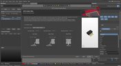
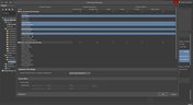
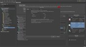
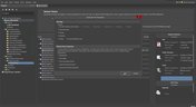
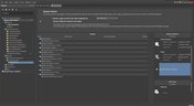
With Altium 365, you can grant permission to teams or users based on the specific needs of a project. We have expanded Altium 365’s file-sharing setting, giving you more granular control over who can download source files and reshare projects with others

Read More
Use your DRCs
Blog • Apr 7, 2022
Design Rule Checking in the PCB Design Workflow

Any time you design a PCB, and you want to turn it into a real product, you will have to make sure the design obeys the constraints within the standard PCB manufacturing process. This imposes multiple rules on any design, and ECAD software will enforce design rules as you create the board to ensure you obey these important constraints. Make sure you enforce the right design rules at the beginning of the PCB design workflow 

Read More
How to select high frequency materials
Blog • Apr 5, 2022
Best Practices for High-Frequency PCB Material Selection

High frequency PCB design can seem esoteric, and I've heard many an engineer describe it as "black magic"! The subject is also a bit confusing, especially once someone asks which frequencies could be reasonably considered "high". Before you do anything inside the layout for a high-speed or RF PCB, you will need to pay attention to the materials being used in the board. If you're unsure which high frequency PCB materials you should use, then keep reading to learn more.

Read More
PCB Noise Reduction
Blog • Mar 31, 2022
PCB Noise Reduction: Do You Need Isolation, Shielding, or Filters?

Of all the noise and operational challenges designers face in their PCBs, there is one overarching problem that is arguably most popular: electronic noise. It could originate as an SI/PI problem, it could possibly arise from some external source, or it could be good old-fashioned crosstalk! These tend to fall into three categories: adding shielding, doing something to create isolation, or placing filters. Let's look at all of these as they tend to be the default solution set when confronted with many noise problems.

Read More
What’s New in Altium 365
Blog • Mar 29, 2022
What’s New in Altium 365: Version Control for Hardware, Layer Stackup in Web Viewer, and SOC 2 Type 1 Certification

In February, we hit a new record in the number of users on the platform. The Altium 365 user community is now 20,000 strong! You can now migrate from an external version control system to Altium 365 preserving the history of commits. We also received the SOC 2 Type 1 certification from KPMG, made layer stack available in the web viewer, and added the brand new capability to track tasks in the context of your design project. Keep reading to learn more!

Read More
Electronic Design to Delivery Index
Blog • Mar 24, 2022
Introducing Spectra's Electronic Design to Delivery Index

Get a cohesive view of supply chain market conditions, stay on top of trends, and avoid disruption with this free, monthly report from Spectra.

Read More
Rigid-Flex in Altium Designer
Blog • Mar 22, 2022
Support for Rigid-Flex in Altium Designer

Rigid-flex in Altium Designer starts with designing a manufacturable PCB layer stack complete with via transitions and any calculated impedance requirements. Flex sections also need to be placed in the layer stack before moving into the PCB layout. Once inside the PCB editor, bending lines can be clearly defined in the PCB layout, and these can be visualized in Altium Designer's 3D PCB design tools. Keep reading to see how Altium Designer supports your flex and rigid-flex designs.

Read More
Specifying your stackup
Blog • Mar 17, 2022
Communicating PCB Layer Stackup Needs to Manufacturers

In the business of PCB design, communicating needs to manufacturers and vendors is a top priority. The context of our requests is sometimes lost either by not providing the correct information, not listing enough information, or not giving any information. Although the experienced PCB designer can take steps to specify everything they want to see in their PCB stackup, eventaully the manufacturer will handle that decision in an effort to balance available materials with processing capabilities and yield.

Read More
Risk Vs. Reward
Blog • Mar 15, 2022
Risk Vs. Reward

During the recent IPC APEX expo, there was a lot of discussion about SAP, or semi-additive PCB processes.  As with any new technology adoption there were people that are excited to jump right in and start designing with much finer feature sizes and work through the inevitable changes to the traditional thought process. Others are in a "let’s wait and see" mode and of course there are a few skeptics there as well, so keep reading to learn more.

Read More
Parasitic Extraction for your traces
Blog • Mar 10, 2022
Parasitic Extraction with an Electromagnetic Solver in PCB Routing

Parasitic extraction: the integrated circuit design community must grapple with this task on a daily basis, especially once gate features are reduced below ~350 nm and chips run at high switching speeds. The PCB community also has to deal with this idea in order to better design power delivery networks, interconnects with precise impedance, and properly quantify crosstalk and coupling mechanisms.

Read More
PCB
Blog • Mar 8, 2022
Ebook: PDN Simulation and Analysis Guide

Most designers don’t realize they need to worry about power integrity until they have a power integrity problem. Other designers might build boards that can’t handle the demands of modern digital and high frequency components, and they may not realize the problems that lurk in their power delivery network (PDN). Although the basic concepts involved in designing for power integrity are well-known, myths about power integrity abound, and designers need tools to help them evaluate and qualify power integrity in a PDN.

Read More
Ferrites in PDN Simulation
Blog • Mar 3, 2022
Ferrite Beads and Transfer Impedance in a PDN Simulation

The use of ferrites in a PDN is one design recommendation that is fraught with unclear guidance and over-generalized recommendations. If you see an application note or a reference design that recommends placing a ferrite in a PDN, should you follow this in your specific design, or should you ignore this and focus on adding capacitance? 

Read More
PCB Design Outputs
Blog • Mar 1, 2022
Overview of PCB Design Output Files

Before your board can be put into production and prepared for assembly, you have to generate a set of files that assist your manufacturer. These are your PCB design output files, also known as manufacturing files, fabrication data, assembly files, and a host of other names. Before you send your design file off to a manufacturer in an email, make sure to get a list of their required fabrication and assembly files first. If you’re a new designer, take some time to read over the basic PCB manufacturing file extensions below.

Read More
How transformers work
Blog • Feb 24, 2022
Transformer Theory Made Simple

Transformers can provide very effective signal isolation and are used to manipulate AC voltage and current levels. They can achieve all this with a greater than 95% power efficiency, which is why we commonly see them used in bench power supplies, audio gear, computers, kitchen appliances, and wall-warts. However, transformer theory can be unintuitive and in this article we answer on questions about them

Read More
Take advantage of the VCS-based workflow in Altium 365
Blog • Feb 22, 2022
Using Altium 365 Over Your Vanilla Version Control System

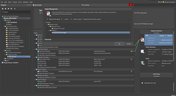
There are all sorts of version control systems (VCS) out there that people have been using with their PCB design software. As discussed in Why Use a Version Control System, we looked at different options ranging for local hard drive storage to sophisticated online revisioning systems. In this article we will be reviewing the differences between a standard VCS and Altium 365.

Read More
  • Show More
Tag (field_common_tag)
Embedded thumbnail for Snapping When Creating Polygons
How to use Snapping • Oct 23, 2020
Snapping When Creating Polygons

When creating polygons you can use snap points to form fit your polygons to the exact size and shape you need. We’ll show you how to set your snap points, which ones are most helpful for creating polygons, and how to use the same techniques to create keep out and solder mask areas.

Start Watching
Embedded thumbnail for Automatic Symbol Creation in Altium 365
Library Managment • Oct 19, 2020
Automatic Symbol Creation in Altium 365

In order to design your projects, you’ll need a set of components to work with. Although the integration of Octopart with Altium Designer gives us a large repertoire of components, you simply can’t have access to every component model in the world. We’re going to create a component in the Altium 365 workspace with the Symbol Creation Wizard.

Start Watching
Embedded thumbnail for Creating Differential Pairs in the PCB
How to Work with Differential Pairs • Aug 21, 2020
Creating Differential Pairs in the PCB

Learn how to create differential pairs in the PCB.

Start Watching
Embedded thumbnail for From The Beatles to the PCB - VOX Story
Success Stories • Aug 19, 2020
From The Beatles to the PCB - VOX Story

Dave Clarke, R&D manager for VOX, walks us through his story of designing VOX amplifiers for electronic instruments as well as his love for music and electronics design. Be sure to subscribe to the Altium Stories channel to stay updated on new videos. Altium LLC is accelerating the pace of innovation through electronics. From individual inventors to multinational corporations, more PCB designers and engineers choose Altium software to design and realize their ideas. 

Start Watching
Embedded thumbnail for Creating PCB Mounting Holes
• Jul 29, 2020
Creating PCB Mounting Holes

Our PCB must somehow be assembled into the final drone assembly. This will be achieved by attaching our PCB to the motherboard connector and by special mounting racks, which requires precise positioning of the two mounting holes on the PCB.

Start Watching
Embedded thumbnail for Working with PCB Keepouts
• Jul 24, 2020
Working with PCB Keepouts

When working in the PCB, there may be specific areas that you would want to prevent the presence of certain objects, such as vias, tracks or copper regions. All of this can be realized in Altium Designer by using the Keepouts feature.

Start Watching
Embedded thumbnail for Local PCB Library & Footprint Creation
Library Managment • Jul 22, 2020
Local PCB Library & Footprint Creation

We’ve already looked at how to create a footprint from scratch, but with the help of the IPC Footprint Wizard, you can create any IPC compliant component by entering a bit of information which is what we’ll be covering.

Start Watching
Embedded thumbnail for Manual Footprint Creation with Altium 365
Library Managment • Jul 22, 2020
Manual Footprint Creation with Altium 365

A footprint or land pattern represents the real-world copper or through-hole component pads that get mounted on the board. We’re going to cover nearly everything that’s needed to create a footprint from scratch and add it to our USB component that’ll be stored in our Altium 365 workspace.

Start Watching
Embedded thumbnail for Local Library and Symbol Creation
Library Managment • Jul 22, 2020
Local Library and Symbol Creation

In the last video, we created a component with a schematic symbol stored in the Altium 365 workspace. Now, we’re going to cover the process of creating a local schematic library with a schematic symbol for our Workspace.

Start Watching
Embedded thumbnail for Generating and Storing Outputs
• Jun 23, 2020
Generating and Storing Outputs

Once our manufacturing and assembly outputs have been configured, we’re ready to generate these outputs that will be stored in the project folder and ready to be sent out to manufacturing.

Start Watching
Embedded thumbnail for Preparing Assembly Outputs
• Jun 23, 2020
Preparing Assembly Outputs

Once you've looked at the fabrication outputs for your PCB, it is time to look at the files needed for the Assembly process. This includes Assembly Drawings, Pick & Place files, and more.

Start Watching
Embedded thumbnail for Preparing Fabrication Outputs
• Jun 23, 2020
Preparing Fabrication Outputs

The files generated in this section are going to be sent to the PCB manufacturer, where they’ll be used to create the bare board. There are a few different files that need to be generated such as Gerbers, NC Drill files, and more.

Start Watching
Embedded thumbnail for Preparing Documentation Outputs
• Jun 23, 2020
Preparing Documentation Outputs

Aside from manufacturing and assembly outputs, you’ll likely want to generate some design documentation as well. We’ll configure outputs for some schematic prints and a bill of materials.

Start Watching
Embedded thumbnail for Creating an Outjob File
• Jun 23, 2020
Creating an Outjob File

Learn how to create documentation for the PCB manufacturer and assembly house. These files can now be generated individually, but it’s much faster and easier to use the OutJob file to output all the files in a central location.

Start Watching
Embedded thumbnail for Design Review Use Case
Discovering Altium 365 • Jun 19, 2020
Design Review Use Case

Design reviews are critical to being successful. Capture design discussions through contextual commenting in the web browser or in Altium Designer to ensure feedback is recorded and actioned effectively.

Start Watching
Embedded thumbnail for Resolving Errors in the PCB
• Jun 17, 2020
Resolving Errors in the PCB

We’ve looked at how to set up the Design Rule Checker to help us analyze our PCB design errors. Now it’s time to resolve these errors and prep our design to start generating output files.

Start Watching
  • Show More
Tag (field_common_tag)
Altium Enterprise
On-Demand Webinar • May 10, 2025
Streamline your customer relation with Altium 365 Enterprise
Join our webinar designed for engineers and users in EMS companies
Watch Now
PCB
On-Demand Webinar • May 1, 2025
Altium Designer Overview
Altium Designer is the #1 PCB design tool for a reason. Join us for this live webinar and get an inside look at Altium’s world-class PCB design solution. See for yourself why design teams around the globe are making the switch to Altium Designer. Register now!
Watch Now
Enterprise
On-Demand Webinar • Apr 25, 2025
Altium Customization with Scripting or Low-Code
See how scripting, low-code, no-code, and API integrations can help you work more efficiently—without extra setup or complex systems.
Watch Now
A365 Webinar: Altium BOM Portal - From PCB Design to Parts Ordering in Minutes
On-Demand Webinar • Apr 21, 2025
Altium 365 BOM Portal - From PCB Design to Parts Ordering in Minutes
Join us to learn how to reduce sourcing time by up to 70% using Altium 365 BOM Portal.
Watch Now
April 2025 COM Webinar
On-Demand Webinar • Apr 17, 2025
Advanced xSignal and Impedance Control Techniques
We are hosting a free webinar on advanced xSignal configuration and impedance control techniques in Altium Designer to help you tackle signal integrity challenges. Register now to enhance your design skills.
Watch Now
Altium Enterprise
On-Demand Webinar • Mar 25, 2025
Unlocking the full potential of your design team with Altium's enterprise solution
See how Altium's enterprise solution can help you meet your electronic product design goals
Watch Now
Transmission line
On-Demand Webinar • Mar 4, 2025
Optimizing Layer Stackup and Impedance for High-Speed PCB Design
Learn how to master the layer stack manager to efficiently create stackups, manage materials, and ensure optimal design performance.
Watch Now
Harness design
On-Demand Webinar • Mar 2, 2025
Design Smarter - Harness, Multi-board, and MCAD CoDesign in Action
Discover how the latest Harness, Multi-board, and MCAD CoDesign tools can revolutionize your PCB design workflow.
Watch Now
ADv25
On-Demand Webinar • Jan 30, 2025
6 Reasons to Switch Design Tools
Come see how Altium Designer, the industry standard for PCB design, combined with Altium 365 delivers the world’s first connected PCB design experience.
Watch Now
PCB CoDesign
On-Demand Webinar • Jan 29, 2025
Level Up Your Team's Productivity with Altium
Discover how to create an efficient, collaborative, and transparent design process for your team!
Watch Now
Assembly variants
On-Demand Webinar • Jan 9, 2025
Designing with Assembly Variants
Join us to learn best practices and get into the details about setting up variants in your designs and speeding up your project development.
Watch Now
Single layer PCB
On-Demand Webinar • Jan 8, 2025
Optimized for Success - Advanced PCB Features in Altium Designer
This webinar will show you how to use the latest PCB Layout, signal integrity analysis, and component management design tools in Altium Designer.
Watch Now
Rigid flex
On-Demand Webinar • Dec 19, 2024
How To Use Modern Rigid-Flex Substrates
Join us in this webinar where we’ll go over how you can easily create your own flex design.
Watch Now
Power Analyzer
On-Demand Webinar • Oct 29, 2024
Power Integrity Made Simple
Power Analyzer by Keysight in Altium Designer makes it easy to resolve PDN issues that arise during the board design process within a unified design environment.
Watch Now
Electronic Component Traceability
On-Demand Webinar • Oct 25, 2024
Ensuring Electronic Component Traceability From Idea to Innovation
Watch the webinar to learn how to achieve full transparency, improve collaboration, and ensure compliance throughout your entire supply chain—whether you are sourcing domestically or abroad.
Watch Now
Why Altium Designer is Your Next Step for PCB Design
On-Demand Webinar • Oct 24, 2024
Why Altium Designer is Your Next Step for PCB Design
Join us to see how moving to Altium Designer can enable resilient and scalable designs while streamlining your entire workflow.
Watch Now
  • Show More
Tag (field_common_tag)
Loading
Loading...
Share link
Share with
Search by Update
Version
Update
25 26 24 23 22
25.0 25.1 25.2 25.3 25.4 25.5 25.6 25.7 25.8 25.9
26.1 26.2
24.10 24.9 24.8 24.7 24.6 24.5 24.4 24.3 24.2 24.1 24.0
23.11 23.10 23.9 23.8 23.7 23.6 23.5 23.4 23.3 23.2 23.1 23.0
22.11 22.10 22.9 22.8 22.7 22.6 22.5 22.4 22.3