
Main navigation

  • Home
  • Discover
  • Learning Center
  • What’s New

Second main navigation

  • Altium Community
  • Support
  • Documentation
×

Results

  • Updates
  • Blog 570
  • Video 539
  • Webinar 86
  • Playlist 53
Filters:
Tag (field_common_tag)
Embedded thumbnail for Altium Training - Navigating Schematics: Schematic Preference Settings for Navigation
Altium Training • Nov 3, 2025
Altium Training - Navigating Schematics: Schematic Preference Settings for Navigation

Unlock smarter design navigation in Altium! Learn how to customize navigation preferences to boost your design insight and visualize connectivity like never before. In this video, we’ll explore Design Insight settings, interactive connectivity hover features, and quick thumbnail navigation between schematic sheets. All designed to make your workflow faster, clearer, and more intuitive.

Start Watching
Blog • Oct 30, 2025
What Is BOM Management? A Practical Guide to Avoiding Costly Part Mismatches

From design to production, effective Bill of Materials (BOM) management is critical to ensuring smooth collaboration between engineering, procurement, and manufacturing teams. In this practical guide, we break down proven strategies for structuring, maintaining, and synchronizing your BOM to prevent costly mistakes and accelerate time-to-market.

Read More
Blog • Oct 29, 2025
Requirements Portal Introductory Tutorials

This series of guided demos shows how the Altium Requirements Portal transforms scattered requirement spreadsheets and emails into traceable, version-controlled data that stays aligned with your PCB design efforts.

Read More
Embedded thumbnail for PCB Design Tools for Every Team Size: Altium's New Approach
How-To's • Oct 28, 2025
PCB Design Tools for Every Team Size: Altium's New Approach

Explore how Altium is transforming PCB design with software solutions built for teams of every size. In this exclusive PCB West 2025 interview, Justin Sears highlights the key distinctions between Altium Develop and Altium Agile helping you identify the ideal platform for your design needs.

Start Watching
Blog • Oct 27, 2025
Bridging the Gap: When to Use Rigid-Flex Instead of Flex & Connector

Discover when a rigid-flex PCB is a better choice than a separate flex circuit and connector, especially for designs requiring compact packaging, repeated motion or high reliability. The article emphasizes that although rigid-flex needs more upfront planning and fabrication collaboration, it often pays off in simpler assemblies and improved performance.

Read More
Embedded thumbnail for PCB Design: Sequential Lamination vs Sub-Lamination
How-To's • Oct 23, 2025
PCB Design: Sequential Lamination vs Sub-Lamination

Explore the key distinctions between sequential lamination and sub-lamination techniques, and learn how each approach influences microvia placement, board complexity, and design flexibility in high-density interconnect (HDI) circuit board fabrication.


Start Watching
Blog • Oct 22, 2025
Bridging Mechanical and Electrical Teams for Smarter Automotive Design

As vehicles evolve into advanced electronic systems, the separation between electrical and mechanical design teams becomes a critical bottleneck. This article explores how synchronized ECAD–MCAD workflows help automotive projects move faster, reduce rework and maintain design integrity.

Read More
Embedded thumbnail for PCB Design Review: Power Meter Layout Deep Dive
How-To's • Oct 21, 2025
PCB Design Review: Power Meter Layout Deep Dive

Gain practical insights into PCB design with an in-depth power meter project review, covering parameter optimization, BOM control, and IPC-compliant high-voltage spacing.

Start Watching
Blog • Oct 20, 2025
Via Structures: Designing for Reliability, Not Just Density

We all want to pack more into our PCB designs, but the smallest via isn’t always the smartest one. Dive in to learn how picking the right structure can save you headaches down the line.

Read More
Embedded thumbnail for Drawing Tools for Pro Schematics in Altium
How-To's • Oct 16, 2025
Drawing Tools for Pro Schematics in Altium

In our brand-new tutorial, you’ll learn how to create professional-looking schematics in Altium using built-in drawing tools and features. We’ll show you how to add custom title blocks, revision histories, tables of contents, block diagrams, and color schemes to make your schematics stand out.

Start Watching
Blog • Oct 15, 2025
How Structural Electronics Enables 3D, Flexible, and Wearable Integration

Structural electronics integrates electronic functionality directly into the physical structure of a product, eliminating the need for traditional circuit boards. This article examines how advances in materials, additive manufacturing, and flexible substrates are enabling compact, 3D, and wearable systems with enhanced performance and design freedom.

Read More
Embedded thumbnail for 3 GHz RF Amplifier Deep Dive
How-To's • Oct 14, 2025
3 GHz RF Amplifier Deep Dive

Check out our design review of a 3.6 GHz RF amplifier! This in-depth analysis highlights schematic issues, PCB layout challenges, and key RF design principles to help you build better high-frequency circuits.

Start Watching
Blog • Oct 9, 2025
Beyond Traces: Why Soldermask May Be the Critical Factor in Ultra HDI

In ultra-HDI designs, soldermask is no longer a passive coating but a pivotal element that can determine manufacturability. This article explores why mask registration, resolution, and feature tolerances become critical as line spacings shrink below 50 µm.

Read More
Embedded thumbnail for The Right Way to Use SIG/GND/PWR/SIG Stackups
How-To's • Oct 8, 2025
The Right Way to Use SIG/GND/PWR/SIG Stackups

Find out how to properly implement signal-ground-power-signal stackups in 4-layer PCB designs. Check out our tutorial from Zach Peterson, where he explains when to use dedicated power layers, how to route signals correctly over split power planes, and common mistakes to avoid for optimal EMI performance and signal integrity.

Start Watching
Blog • Oct 7, 2025
How ECAD-MCAD Co-Design Supports Aerospace Reliability and Compliance

When the margin for error is nearly zero, aerospace engineering demands a design process that’s seamless across all domains. Here, we explore how ECAD-MCAD co-design delivers an integrated workflow that supports first-pass success and compliance with strict aerospace standards.

Read More
Embedded thumbnail for Altium Training - Design Environment: Documents and Panels
Altium Training • Oct 6, 2025
Altium Training - Design Environment: Documents and Panels

In our new tutorial, we explore different panel display modes, including docked, floating, and tabbed grouping arrangements. Effective panel management is essential for creating an efficient design environment tailored to your specific workflow requirements.

Start Watching
  • Show More
Tag (field_common_tag)
Why the Principles Are Sound, but the Tactics Need a Re-Think
Blog • Feb 26, 2024
What Most Agile "Gurus" Get Wrong About Hardware Development

Explore common myths about Agile hardware development and learn how to adapt Agile principles for hardware projects.

Read More
Blog • Feb 23, 2024
Design Phase – Lid Assembly Electronics Part 2

We are going deeper into lid assembly electronics in our Open Source Laptop project. In this chapter we will tackle the PCB design of the webcam board and show you how to deal with some expected challenges, such as overall small form factor of the board or breaking out the microscopic webcam image sensor.

Read More
Commercial Altium 365 vs Altium 365 GovCloud Comparison
Blog • Feb 20, 2024
Compare Commercial Altium 365 vs Altium 365 GovCloud

If you're trying to understand how commercial Altium 365 differs from Altium 365 GovCloud, you're in the right place. Click to grasp the unique features of each.

Read More
Agile Hardware Development
Blog • Feb 19, 2024
5 Ways Hardware Development Is Just… Different

Explore the challenges and strategies of implementing Agile methodology in electronics hardware development. Understand key differences between hardware and software development within the Agile framework.

Read More
Blog • Feb 13, 2024
Flexible Circuit Assembly: Thinking Through Component Placement

The flexible circuits are ideal for applications where a thin, small, and lightweight PCB is needed. However, in such cases, challenges in assembly and fabrication often arise. This article delves into these challenges, focusing on component selection and placement and how they can significantly impact the performance of the flexible circuit in its intended application.

Read More
Blog • Feb 9, 2024
Coding Your Own Networked Test Equipment

Have you ever performed manual tests? If your answer is yes, you're likely aware of how laborious and time-consuming the entire process can be. Allow us to introduce you to the realm of test equipment automation. Our new step-by-step guide empowers you to write code that seamlessly configures your networked test equipment, all from the convenience of your computer.

Read More
Blog • Feb 6, 2024
Pi.MX8 Project – Schematic structure and component placement

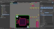
We are advancing with our brand new Pi.MX8 Project. In this chapter, we delve deeper into two crucial aspects: the overall schematic and component placement on the PCB board. Don't hesitate to check it out. Additionally, you can follow this project through our workspace; the link is provided within the article.

Read More
Blog • Jan 31, 2024
Redefine PCB Boundaries with HDI Design

Dive into the world of High-Density Interconnect (HDI) design to enhance your projects. Explore heightened signal integrity, improved reliability, and the seamless integration of advanced technologies - all within compact and lightweight designs. Discover more about HDI on our updated feature page.

Read More
OrCAD Design Collaboration in Altium 365
Blog • Jan 29, 2024
OrCAD Design Collaboration in Altium 365

Ready to start collaborating on your OrCAD projects in a multi-CAD environment? Check how you can use Multi-CAD File Support in Altium 365 in practice.

Read More
Blog • Jan 25, 2024
The Critical Role of Constraint-Based PCB Design in Modern Electronics

A constraint-based approach to PCB design is crucial in today's electronics industry. This article delves deeper into this complex and interesting topic, exploring various types of constraints, their advantages, and providing guidance on implementing them into your PCB design process.

Read More
Blog • Jan 23, 2024
Pi.MX8 Project – Introduction and Overview

Do you have extensive knowledge about the Pi.MX8 module? We're excited to introduce a new series of articles focusing on an innovative approach to utilizing this module. In this inaugural chapter, we provide insights into the preparation for this project and detail the elements that will be used.

Read More
Connect Procurement and Engineering Cover Photo
Blog • Jan 22, 2024
How to 'Shift Left' and Connect Procurement and Engineering? Altium 365 BOM Portal Step-by-Step

Learn why BOM management is critical for both procurement managers and electronic engineers. Altium 365 BOM Portal helps to bridge the gap between these worlds. Discover how!

Read More
Blog • Jan 10, 2024
Altium 365 Assembly Assistant: Available Now in the Altium Store

Happy New Year! 🎉 We are thrilled to announce that the Altium 365 Assembly Assistant is now officially released and available for direct purchase through the Altium Store.

Read More
Blog • Jan 9, 2024
Simple Documentation for Hand PCB Assembly

Creating documentation for hand PCB assembly does not prevent the same documentation from being utilized to assist in automated PCB assembly. Learn more about the optimal format for this data to enhance both your hand PCB assembly and overall assembly processes.

Read More
Blog • Jan 8, 2024
Constraint Manager: Precision in Every Detail

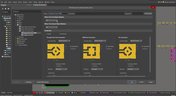
Explore the powerful features of Altium Designer 24! Experience Constraint Manager and revolutionize your PCB design with reusable constraint sets, schematic-to-board rule transition, easy class and differential pair grouping, and more.

Read More
Accelerate Last-Minute Design Changes Cover Photo
Blog • Dec 21, 2023
Accelerate Last-Minute Design Changes with Altium 365

Curious about how to solve production blockers before they derail your product launch? Explore how Altium 365® can help you swiftly manage last-minute design changes.

Read More
  • Show More
Tag (field_common_tag)
Embedded thumbnail for Performing Board DRC
• Jun 16, 2020
Performing Board DRC

Design rules are crucial to a PCB’s overall design and performance. It’s just as important to adhere to these rules and ensure that we didn’t overlook any unconnected nets or short circuits. This is why we need to run a Design Rule check.

Start Watching
Embedded thumbnail for Placing a Custom 3D Body in 3D View
• Jun 16, 2020
Placing a Custom 3D Body in 3D View

With the help of the 3D view, it is possible to view a PCB design from all sides, to check on component placement, silkscreen alignment, and many other visual aspects.

Start Watching
Embedded thumbnail for Silkscreen Placement
• Jun 16, 2020
Silkscreen Placement

The silkscreen layer is the layer on which we print any visual text or symbols on our PCB. With the help of this silkscreen layer, we can print our component designators, pin placement, and more.

Start Watching
Embedded thumbnail for Working with Polygon Pours
• Jun 16, 2020
Working with Polygon Pours

When working with common signals, the current levels are usually quite minimal, but when working with power nets it’s not uncommon to see current levels of a few amps. One of the reasons to use polygons is to maintain the quality and reliability of the power supply system.

Start Watching
Embedded thumbnail for Routing Post Processes
• Jun 16, 2020
Routing Post Processes

Depending on how you routed your board, it may be a time-consuming process to fix these manually. So we’ll dive into Route Glossing a little more, along with an automated way to retrace pre-existing routes.

Start Watching
Embedded thumbnail for PCB Layout Cleanup
• Jun 16, 2020
PCB Layout Cleanup

After the board has been routed, it’s almost certain that you’ll need to either move, delete, or adjust some traces. We’ll be looking at a few basic methods to easily modify and remove traces in our design.

Start Watching
Embedded thumbnail for Differential Pair Routing
• Jun 16, 2020
Differential Pair Routing

Routing Differential Pairs is similar to routing single traces, but there are additional rules and guidelines to follow that will help you avoid signal integrity problems.

Start Watching
Embedded thumbnail for Introduction to Routing
• Jun 16, 2020
Introduction to Routing

We’ve looked at different routing behaviors and options that we can change to make routing much easier. So we’re going to dive into the basics of routing and how these settings and routing modes can be applied.

Start Watching
Embedded thumbnail for Defining the Layer Stackup
• Jun 10, 2020
Defining the Layer Stackup

The PCB is designed and formed as a stack of layers and the definition of the PCB layer stack is a critical element of successful printed circuit board design. In Altium Designer, the Layer Stack Manager is used to develop the printed circuit board internal design including layer-pairing, careful via design, any back drilling requirements, rigid/flex requirements, copper balancing, layer stack symmetry, and material compliance. This video guides you through creation of a layer stackup, adding the necessary layers, as well as adding an impedance profile.

Start Watching
Embedded thumbnail for Searching for Errors in Schematic
• May 20, 2020
Searching for Errors in Schematic

Searching for Errors: Errors and mistakes happen to everyone - from beginners to professionals. So we always preach how it is paramount for your design to be validated before pushing it to the PCB. But luckily it’s pretty easy to find and analyze any errors using Altium Designer. We’ll take a look at how to find and analyze errors in your schematic.

Start Watching
Embedded thumbnail for Creating Net Classes
• Jun 2, 2020
Creating Net Classes

A Net Class is a collection of nets that can be used for creating a targeted design rule. So for example, you may want all power and ground nets to have a minimum track width to handle a specific current rating. So we’ll show you how to assign these nets to a NetClass. 

Start Watching
Embedded thumbnail for Configuring Design Rules - Part 2
• May 14, 2020
Configuring Design Rules - Part 2

Altium Designer uses the concept of Design Rules to define the requirements of a design. These rules collectively form an instruction set for the PCB Editor to follow. They cover every aspect of the design - from routing widths, clearances, plane connection styles and so on. With a well-defined set of design rules, you can successfully complete board designs with varying and often stringent design requirements.

Start Watching
Embedded thumbnail for Routing Modes and Setup
• May 12, 2020
Routing Modes and Setup

Most of you know that routing can be a time consuming process, but it doesn’t have to be a daunting task if you have the right tools. So we’ll be looking at what options and settings can help us perfect the art of routing.

Start Watching
Embedded thumbnail for PCB Component Placement
• May 12, 2020
PCB Component Placement

Component placement in the PCB is an important stage of the design process as it sets the precedent for efficient and clean routing. We’ll be diving into different component placement methods along with some tips and tricks that you can use to make this an easy process. 

Start Watching
Embedded thumbnail for Configuring the Basic Rules
• May 12, 2020
Configuring the Basic Rules

Altium Designer uses the concept of Design Rules to define the requirements of a design. These rules collectively form an instruction set for the PCB Editor to follow. They cover every aspect of the design - from routing widths, clearances, plane connection styles and so on. With a well-defined set of design rules, you can successfully complete board designs with varying and often stringent design requirements.

Start Watching
Embedded thumbnail for Snap Options in the PCB
• May 12, 2020
Snap Options in the PCB

When you’re ready to dive into your PCB layout, you’re going to want to configure specific options that’ll help you with routing or component placement. So we’ll look at how Snap Options are used for Grids and Objects.

Start Watching
  • Show More
Tag (field_common_tag)
Altium Enterprise
On-Demand Webinar • May 10, 2025
Streamline your customer relation with Altium 365 Enterprise
Join our webinar designed for engineers and users in EMS companies
Watch Now
PCB
On-Demand Webinar • May 1, 2025
Altium Designer Overview
Altium Designer is the #1 PCB design tool for a reason. Join us for this live webinar and get an inside look at Altium’s world-class PCB design solution. See for yourself why design teams around the globe are making the switch to Altium Designer. Register now!
Watch Now
Enterprise
On-Demand Webinar • Apr 25, 2025
Altium Customization with Scripting or Low-Code
See how scripting, low-code, no-code, and API integrations can help you work more efficiently—without extra setup or complex systems.
Watch Now
A365 Webinar: Altium BOM Portal - From PCB Design to Parts Ordering in Minutes
On-Demand Webinar • Apr 21, 2025
Altium 365 BOM Portal - From PCB Design to Parts Ordering in Minutes
Join us to learn how to reduce sourcing time by up to 70% using Altium 365 BOM Portal.
Watch Now
April 2025 COM Webinar
On-Demand Webinar • Apr 17, 2025
Advanced xSignal and Impedance Control Techniques
We are hosting a free webinar on advanced xSignal configuration and impedance control techniques in Altium Designer to help you tackle signal integrity challenges. Register now to enhance your design skills.
Watch Now
Altium Enterprise
On-Demand Webinar • Mar 25, 2025
Unlocking the full potential of your design team with Altium's enterprise solution
See how Altium's enterprise solution can help you meet your electronic product design goals
Watch Now
Transmission line
On-Demand Webinar • Mar 4, 2025
Optimizing Layer Stackup and Impedance for High-Speed PCB Design
Learn how to master the layer stack manager to efficiently create stackups, manage materials, and ensure optimal design performance.
Watch Now
Harness design
On-Demand Webinar • Mar 2, 2025
Design Smarter - Harness, Multi-board, and MCAD CoDesign in Action
Discover how the latest Harness, Multi-board, and MCAD CoDesign tools can revolutionize your PCB design workflow.
Watch Now
ADv25
On-Demand Webinar • Jan 30, 2025
6 Reasons to Switch Design Tools
Come see how Altium Designer, the industry standard for PCB design, combined with Altium 365 delivers the world’s first connected PCB design experience.
Watch Now
PCB CoDesign
On-Demand Webinar • Jan 29, 2025
Level Up Your Team's Productivity with Altium
Discover how to create an efficient, collaborative, and transparent design process for your team!
Watch Now
Assembly variants
On-Demand Webinar • Jan 9, 2025
Designing with Assembly Variants
Join us to learn best practices and get into the details about setting up variants in your designs and speeding up your project development.
Watch Now
Single layer PCB
On-Demand Webinar • Jan 8, 2025
Optimized for Success - Advanced PCB Features in Altium Designer
This webinar will show you how to use the latest PCB Layout, signal integrity analysis, and component management design tools in Altium Designer.
Watch Now
Rigid flex
On-Demand Webinar • Dec 19, 2024
How To Use Modern Rigid-Flex Substrates
Join us in this webinar where we’ll go over how you can easily create your own flex design.
Watch Now
Power Analyzer
On-Demand Webinar • Oct 29, 2024
Power Integrity Made Simple
Power Analyzer by Keysight in Altium Designer makes it easy to resolve PDN issues that arise during the board design process within a unified design environment.
Watch Now
Electronic Component Traceability
On-Demand Webinar • Oct 25, 2024
Ensuring Electronic Component Traceability From Idea to Innovation
Watch the webinar to learn how to achieve full transparency, improve collaboration, and ensure compliance throughout your entire supply chain—whether you are sourcing domestically or abroad.
Watch Now
Why Altium Designer is Your Next Step for PCB Design
On-Demand Webinar • Oct 24, 2024
Why Altium Designer is Your Next Step for PCB Design
Join us to see how moving to Altium Designer can enable resilient and scalable designs while streamlining your entire workflow.
Watch Now
  • Show More
Tag (field_common_tag)
Loading
Loading...
Share link
Share with
Search by Update
Version
Update
25 26 24 23 22
25.0 25.1 25.2 25.3 25.4 25.5 25.6 25.7 25.8 25.9
26.1 26.2
24.10 24.9 24.8 24.7 24.6 24.5 24.4 24.3 24.2 24.1 24.0
23.11 23.10 23.9 23.8 23.7 23.6 23.5 23.4 23.3 23.2 23.1 23.0
22.11 22.10 22.9 22.8 22.7 22.6 22.5 22.4 22.3