
Main navigation

  • Home
  • Discover
  • Learning Center
  • What’s New

Second main navigation

  • Altium Community
  • Support
  • Documentation
×

Results

  • Updates
  • Blog 571
  • Video 540
  • Webinar 86
  • Playlist 53
Filters:
Tag (field_common_tag)
Embedded thumbnail for Demonstration Altium DISCOVER - Embedded World North America 2025
Embedded World 2025 • Dec 8, 2025
Demonstration Altium DISCOVER - Embedded World North America 2025

Check out our live demo from Embedded World North America 2025 showcasing Altium Discover. In this video, you’ll see how the platform helps reduce sourcing risk, shorten design cycles, and keep projects moving forward with confidence.

Start Watching
Blog • Dec 4, 2025
How to Manage ECAD Libraries for Consistent PCB Layout Design

Strong hardware starts with strong libraries. Discover how disciplined ECAD-library management dramatically improves design consistency and accelerates every stage of your PCB workflow.

Read More
Embedded thumbnail for Altium Agile for Modern Electronics Development - Presentation Embedded World North America 2025
Embedded World 2025 • Dec 3, 2025
Altium Agile for Modern Electronics Development - Presentation Embedded World North America 2025

Watch our presentation from Embedded World North America 2025 to learn how Altium Agile brings structure, visibility, and velocity to modern hardware development. Discover how multidisciplinary teams can eliminate workflow chaos, track progress in real time, and accelerate delivery without compromising quality.

Start Watching
Blog • Dec 2, 2025
High Speed PCB Design Review: Signal Integrity Questions You Should Always Ask

As data rates increase, the risks hidden in your layout grow with them. This quick guide highlights the critical SI checkpoints that can save you from late-stage surprises and redesigns. If you design high-speed boards, you’ll want to read this before your next review.

Read More
Embedded thumbnail for Demonstration Altium DEVELOP - Embedded World North America 2025
Embedded World 2025 • Dec 1, 2025
Demonstration Altium DEVELOP - Embedded World North America 2025

See how Altium Develop empowers engineering teams with fast, cloud-connected PCB design built for modern collaboration. This live demo from Embedded World North America 2025 showcases real-time co-creation, smooth MCAD-ECAD integration, and a design environment that lets you stay focused on what matters building great products.

Start Watching
Blog • Nov 26, 2025
Supplier Negotiation: Turn Market Data Into Your Best Negotiation Tool

Don’t walk into supplier talks blind. Use market data to benchmark quotes, check lead times and uncover alternate parts. This article shows how visibility can shift the balance and de-risk your BOM.

Read More
Embedded thumbnail for From Collaboration to Co Creation – Presentation Embedded World North America 2025
Embedded World 2025 • Nov 25, 2025
From Collaboration to Co Creation – Presentation Embedded World North America 2025

In this Embedded World North America 2025 presentation, learn how Altium enables electrical, mechanical, firmware, sourcing, and manufacturing teams to collaborate seamlessly in real time through shared data, shared context, and shared visibility. Experience how unified workflows reduce rework, speed up decision-making, and empower teams to deliver exceptional products faster.

Start Watching
Blog • Nov 24, 2025
Via-in-Pad in Rigid-Flex Designs: When Space Is Tight, Details Matter

Designing rigid-flex boards is like solving a 3D puzzle of materials, bends and tight spaces, and via-in-pad might just be the piece you need. Dive into how and when to use via-in-pad in rigid-flex designs, and what to watch out for from fabrication to field reliability.

Read More
Embedded thumbnail for PCB Design: Defining Electrical Clearances in High Voltage PCBs
How-To's • Nov 20, 2025
PCB Design: Defining Electrical Clearances in High Voltage PCBs

Unlock the essential principles behind defining electrical clearances for high-voltage PCB designs in our brand-new tutorial. Learn how to apply accurate, layer-specific clearance rules using IPC-2221 standards and harness the full power of Altium’s query system.

Start Watching
Blog • Nov 19, 2025
Wearable Electronics: Innovations, Challenges & Future Trends

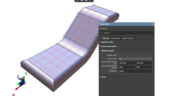
This whitepaper examines how next-generation wearable electronics are evolving through advancements in flexible and rigid-flex design, smart materials, AI, energy innovations, and connectivity. Discover what’s required to transform early prototypes into scalable, reliable products across healthcare, sports, defense, fashion, and enterprise applications.

Read More
Embedded thumbnail for Demonstration Altium AGILE Enterprise - Embedded World North America 2025
Embedded World 2025 • Nov 18, 2025
Demonstration Altium AGILE Enterprise - Embedded World North America 2025

Experience how Altium Agile Enterprise turns complex engineering collaboration into a streamlined, unified workflow. In this live demonstration from Embedded World North America 2025, you’ll see how multi-disciplinary teams can simplify processes, minimize rework, and maintain clear alignment from requirements through release. All within a single, powerful platform.

Start Watching
Blog • Nov 17, 2025
Streamlining Component Selection for Long Product Lifecycles

Electronic parts may now cycle from launch to end-of-life in just a few years, but many systems are expected to serve for 10–20+ years. Here’s how to build a component selection process that aligns engineering, procurement and design for longevity and stability.

Read More
Embedded thumbnail for Highlights from the Altium Booth at Embedded World North America 2025
Embedded World 2025 • Nov 12, 2025
Highlights from the Altium Booth at Embedded World North America 2025

Check out our short recap of Altium’s participation at Embedded World North America 2025 in Anaheim. In the coming weeks, we’ll be sharing a few exciting presentations and demos featuring our new products: Altium Develop, Altium Agile, and Altium Discover.

Start Watching
Blog • Nov 12, 2025
Using ECAD Software to Track Part Availability During PCB Design

As component lead-times extend and obsolescence becomes a persistent threat, PCB projects demand more than schematic capture and layout tools alone. This article details how ECAD software with embedded supply-chain intelligence can: unify engineering and procurement teams; provide visibility into stock levels, lead times and alternates; and enable proactive risk mitigation within the design loop.

Read More
Embedded thumbnail for USB-PD Business Card: Examination & Power Test
How-To's • Nov 10, 2025
USB-PD Business Card: Examination & Power Test

Join us as we explore a PCB business card received at the PCB West Conference. We'll take a closer look under the microscope to examine its intricate components, test its power delivery capabilities, and uncover the engineering marvel behind this tiny device.

Start Watching
Blog • Nov 6, 2025
PCB Design Data Management Tips for Multi-Board Projects

In complex electronic systems, managing data from multiple printed circuit boards can quickly become a logistical challenge. This article outlines a structured workflow for handling both board-level and assembly-level design outputs, ensuring clarity and consistency across fabrication, assembly and product-level documentation.

Read More
  • Show More
Tag (field_common_tag)
electrical circuit with microcontroller
Blog • Dec 27, 2022
Designing Custom Hardware with Microcontrollers

In this article, we’ll look at all that is required to start creating your own custom microcontroller-based hardware designs. You’ll see that there actually isn’t too much to this, as microcontroller manufacturers over the years have tried to make the learning curve less steep and their devices more, and more accessible. This is both from an electrical point of view but also – equally importantly – from a programming point of view.

Read More
high-speed printed circuit board
Blog • Dec 22, 2022
Guide to Low-Dk PCB Materials

If you’ve taken time to learn about PCB material options and layer constructions, you have probably seen the wide range of materials that are available on the market. Materials companies produce laminates with varying Dk values, Tg values, weave styles, CTI values, and mechanical properties to target various applications in the electronics industry.

Read More
freeway in the background of the city
Blog • Dec 20, 2022
Designing for V2X Communication: Wireless Protocols and Standards

If you’re waiting for truly connected cars on a grand scale, there is still a massive amount of work to be done, both on the hardware and software sides. Connected cars can only become a widespread reality once the automotive industry and telecom carriers can decide which protocol will work best for vehicle-to-everything (V2X) communication. PCB designers will then need to step in to create these systems and fit them into a vehicular environment.

Read More
Everything You Need to Know About Stitching Vias
Blog • Dec 15, 2022
Everything You Need to Know About Stitching Vias

This one area of PCB design can be contentious among some designers as it is related to copper pour, which it is often stated is not needed in most designs. Regardless of your feelings about copper pour, stitching vias have important uses in PCBs at low frequencies and at high frequencies.

Read More
IPC-2221 Calculator for PCB Trace Current and Heating
Blog • Dec 13, 2022
IPC-2221 Calculator for PCB Trace Current and Heating

The IPC-2221 standard includes many requirements for printed circuit board design and manufacturability, and there are several online calculators that have been developed based on this standard.

Read More
All About Box Build Assemblies
Blog • Dec 8, 2022
All About Box Build Assemblies

When you’re ready to manufacture a new device at production volume, there are many aspects of the product that must come together. The enclosure, cabling and connectors, embedded software/firmware, and of course the PCBA all have to be considered in totality. There is a quick way to get your product into a usable enclosure, complete with input power and cabling, and with a form factor that fits your PCBA. This overused route to a new product is a box build assembly. 

Read More
Ultra-HDI Technology is Not New
Blog • Dec 6, 2022
Ultra-HDI Technology is Not New

Printed circuit board fabricators have become skilled at manufacturing these technologies and also at understanding the reliability and producibility challenges associated with high-density-interconnect technology. Let’s look at where the PCB industry is at today. 

Read More
Today's PCB Designers Are Driving Electronics Product Design
Blog • Dec 1, 2022
Today's PCB Designers Are Driving Electronics Product Design

What can the industry do to support PCB designers as they continue taking a more active role in product development? Here at Altium, there has been a progressive shift towards looking at the system level and creating tools that get designers more involved throughout the product development process. As the saying goes, over the wall engineering is over… today’s most successful products are built in a collaborative process.

Read More
Phased Array Antenna Design for 5G Applications
Blog • Nov 29, 2022
Phased Array Antenna Design for 5G Applications

As the 5G rollout progresses and researchers continue to discuss 6G, many new 5G-capable products operating in sub-GHz and mmWave bands are reaching the marketplace. Devices that will include a 5G-compatible front-end, whether small stations/repeaters or handheld devices, use phased arrays as high-gain antenna systems to provide high data throughput without losing range at higher frequencies.

Read More
IPC - Vias
Blog • Nov 24, 2022
IPC - Vias

Via protection is an important part of modern PCB design. It provides additional benefits in PCB manufacturing and assembly, increasing the number of acceptable products.

Read More
Power Integrity Analysis in Your PCB Design Software
Blog • Nov 22, 2022
Power Integrity Analysis in Your PCB Design Software

Power integrity problems can abound in modern PCBs, especially high-speed boards that run with fast edge rates. These systems require precise design of the PDN impedance to ensure stable power is always delivered throughout the system.

Read More
Schematic Compare
Blog • Nov 17, 2022
Schematic Compare

A design project doesn’t appear out of nowhere. The design process spreads over time, and project documents change. Schematic documents gradually become more complex, new functional blocks appear, and already finished parts can be modified and updated.

Read More
SPICE
Blog • Nov 16, 2022
Altium Designer 22.11 Update

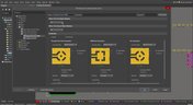
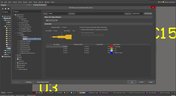
We are happy to announce that the Altium Designer 22.11 update is now available. Altium Designer 22.11 continues to focus on improving the user experience, as well as performance and stability of the software, based on feedback from our users. Check out the key new features in the What's New section on the left side of this window!

Read More
Embedded Capacitance Materials Overview
Blog • Nov 15, 2022
Embedded Capacitance Materials Overview

Capacitance is your friend whenever you need stable power integrity, which is why there is so much focus on decoupling capacitors. While these components are important and they can be used to provide targeted power integrity solutions to certain components, there is one specialty material used to supercharge capacitance in your PCB stackup or package substrate. 

Read More
How To Import Libraries and Manage Components With Altium 365
Blog • Nov 15, 2022
How To Import Libraries and Manage Components With Altium 365

The problems you can experience with components and libraries are endless. These problems are the most significant source of design issues and the biggest reason behind respins, costing companies untold amounts of lost profit annually.
If you want to have a better understanding of how to use Altium 365 to maintain a strong and centralized library that is free of problems and headaches, you may want to consider attending this lecture.

Read More
The High-Speed PCB Stackup Design Challenge
Blog • Nov 10, 2022
The High-Speed PCB Stackup Design Challenge

As much as we would like to build every high speed PCB perfectly, with ideal SI/PI/EMI characteristics, it isn’t always possible due to many practical constraints. Sometimes a stackup can be “good enough,” even for a high-speed PCB. This always comes from the need to balance engineering constraints, functional requirements, and the need to ensure signal and power integrity in a high-speed design, and finally to ensure compliance with EMC requirements.

Read More
  • Show More
Tag (field_common_tag)
Embedded thumbnail for Searching for Errors
• Jun 16, 2020
Searching for Errors

We’ve looked at how to set up the Design Rule Checker to help us analyze our PCB design errors. Now it’s time to resolve these errors and prep our design to start generating output files.

Start Watching
Embedded thumbnail for Performing Board DRC
• Jun 16, 2020
Performing Board DRC

Design rules are crucial to a PCB’s overall design and performance. It’s just as important to adhere to these rules and ensure that we didn’t overlook any unconnected nets or short circuits. This is why we need to run a Design Rule check.

Start Watching
Embedded thumbnail for Placing a Custom 3D Body in 3D View
• Jun 16, 2020
Placing a Custom 3D Body in 3D View

With the help of the 3D view, it is possible to view a PCB design from all sides, to check on component placement, silkscreen alignment, and many other visual aspects.

Start Watching
Embedded thumbnail for Silkscreen Placement
• Jun 16, 2020
Silkscreen Placement

The silkscreen layer is the layer on which we print any visual text or symbols on our PCB. With the help of this silkscreen layer, we can print our component designators, pin placement, and more.

Start Watching
Embedded thumbnail for Working with Polygon Pours
• Jun 16, 2020
Working with Polygon Pours

When working with common signals, the current levels are usually quite minimal, but when working with power nets it’s not uncommon to see current levels of a few amps. One of the reasons to use polygons is to maintain the quality and reliability of the power supply system.

Start Watching
Embedded thumbnail for Routing Post Processes
• Jun 16, 2020
Routing Post Processes

Depending on how you routed your board, it may be a time-consuming process to fix these manually. So we’ll dive into Route Glossing a little more, along with an automated way to retrace pre-existing routes.

Start Watching
Embedded thumbnail for PCB Layout Cleanup
• Jun 16, 2020
PCB Layout Cleanup

After the board has been routed, it’s almost certain that you’ll need to either move, delete, or adjust some traces. We’ll be looking at a few basic methods to easily modify and remove traces in our design.

Start Watching
Embedded thumbnail for Differential Pair Routing
• Jun 16, 2020
Differential Pair Routing

Routing Differential Pairs is similar to routing single traces, but there are additional rules and guidelines to follow that will help you avoid signal integrity problems.

Start Watching
Embedded thumbnail for Introduction to Routing
• Jun 16, 2020
Introduction to Routing

We’ve looked at different routing behaviors and options that we can change to make routing much easier. So we’re going to dive into the basics of routing and how these settings and routing modes can be applied.

Start Watching
Embedded thumbnail for Defining the Layer Stackup
• Jun 10, 2020
Defining the Layer Stackup

The PCB is designed and formed as a stack of layers and the definition of the PCB layer stack is a critical element of successful printed circuit board design. In Altium Designer, the Layer Stack Manager is used to develop the printed circuit board internal design including layer-pairing, careful via design, any back drilling requirements, rigid/flex requirements, copper balancing, layer stack symmetry, and material compliance. This video guides you through creation of a layer stackup, adding the necessary layers, as well as adding an impedance profile.

Start Watching
Embedded thumbnail for Searching for Errors in Schematic
• May 20, 2020
Searching for Errors in Schematic

Searching for Errors: Errors and mistakes happen to everyone - from beginners to professionals. So we always preach how it is paramount for your design to be validated before pushing it to the PCB. But luckily it’s pretty easy to find and analyze any errors using Altium Designer. We’ll take a look at how to find and analyze errors in your schematic.

Start Watching
Embedded thumbnail for Creating Net Classes
• Jun 2, 2020
Creating Net Classes

A Net Class is a collection of nets that can be used for creating a targeted design rule. So for example, you may want all power and ground nets to have a minimum track width to handle a specific current rating. So we’ll show you how to assign these nets to a NetClass. 

Start Watching
Embedded thumbnail for Configuring Design Rules - Part 2
• May 14, 2020
Configuring Design Rules - Part 2

Altium Designer uses the concept of Design Rules to define the requirements of a design. These rules collectively form an instruction set for the PCB Editor to follow. They cover every aspect of the design - from routing widths, clearances, plane connection styles and so on. With a well-defined set of design rules, you can successfully complete board designs with varying and often stringent design requirements.

Start Watching
Embedded thumbnail for Routing Modes and Setup
• May 12, 2020
Routing Modes and Setup

Most of you know that routing can be a time consuming process, but it doesn’t have to be a daunting task if you have the right tools. So we’ll be looking at what options and settings can help us perfect the art of routing.

Start Watching
Embedded thumbnail for PCB Component Placement
• May 12, 2020
PCB Component Placement

Component placement in the PCB is an important stage of the design process as it sets the precedent for efficient and clean routing. We’ll be diving into different component placement methods along with some tips and tricks that you can use to make this an easy process. 

Start Watching
Embedded thumbnail for Configuring the Basic Rules
• May 12, 2020
Configuring the Basic Rules

Altium Designer uses the concept of Design Rules to define the requirements of a design. These rules collectively form an instruction set for the PCB Editor to follow. They cover every aspect of the design - from routing widths, clearances, plane connection styles and so on. With a well-defined set of design rules, you can successfully complete board designs with varying and often stringent design requirements.

Start Watching
  • Show More
Tag (field_common_tag)
 Preventing Obsolescence Before It Hits
On-Demand Webinar • Jun 12, 2025
Proactive Lifecycle Management: Preventing Obsolescence Before It Hits
Take the first step toward eliminating avoidable delays and costly redesigns. Don't miss it and register now!
Watch Now
Integrating Requirements June 2025 Webinar
On-Demand Webinar • May 28, 2025
Integrating Requirements into Your PCB Design Workflow
Join our webinar where you will learn about integrated requirements tools who can help you eliminate late-stage design changes, AI support through system requirements and integration of design requirements directly in PCB Design. Don't miss it, register now!
Watch Now
A365 Webinar
On-Demand Webinar • Apr 23, 2025
Collaborative Design Review: Ensuring Quality from Schematics to Supply Chain
Join our live webinar to learn how Altium 365 accelerates collaboration, standardizes workflows, and ensures design integrity to mitigate risks and accelerate time to market.
Watch Now
Webinar: From Prototype to Production: Optimizing BOM Costs Without Compromising Quality with Part Analytics
On-Demand Webinar • Apr 22, 2025
From Prototype to Production: Optimizing BOM Costs Without Compromising Quality with Part Analytics
Learn how to reduce production BOM costs without redesign, explore techniques to consolidate part demand for volume savings, and discover case examples from supply chain teams that increased sourcing process efficiency by up to 97%.
Watch Now
Streamlining Team Collaboration
On-Demand Webinar • Apr 17, 2025
Streamlining Team Collaboration in Industrial PCB Projects
Join us for our upcoming webinar to discover how Altium Designer and Altium 365 can transform your team’s collaboration and take your PCB design projects to the next level. Attend for a chance to win free access to the Altium 365 Training Bundle.
Watch Now
Component management
On-Demand Webinar • Apr 10, 2025
Ensure Best Designs with Professional Library Management
In this webinar, you'll discover how Altium Designer facilitates robust component management, including adding part choices to mitigate supply chain risks and leveraging Altium 365 managed components.
Watch Now
April 2025 Webinar Cover
On-Demand Webinar • Apr 9, 2025
Component Selection in Altium Designer: Making Data-Driven Decisions with Data Integrations
Improve component selection with real-time data insights in Altium 365! Join our live webinar to optimize your PCB development. Sign up now!
Watch Now
Live Webinar
TEST
Jan
30
English
2:41 AM, PST
Jan
31
English
12:00 PM, CET
Jan
31
German
3:00 PM, CET
Register Now
Altium Agile
Live Webinar
Altium Agile Teams - Sneak Peek
Get a first glimpse into this new Electronic Product Development Platform.
Jan
21
English
3:00 PM, CET
Jan
21
German
10:00 AM, CET
Jan
22
Italian
10:00 AM, CET
Jan
22
French
3:00 PM, CET
Jan
22
Spanish
3:00 PM, CET
Register Now
Altium Platform
On-Demand Webinar • Nov 21, 2025
Altium Platform - A foundation to meet your & your company’s targets
Discover how the Altium platform makes multidisciplinary cooperation easy and efficient.
Watch Now
Harness design
On-Demand Webinar • Nov 17, 2025
From single PCB to Harnessed Product
Discover how to streamline PCB-to-harness design with Altium’s powerful tools and boost collaboration across disciplines.
Watch Now
3D-MID Design
On-Demand Webinar • Oct 20, 2025
3D-MID Design in Altium
Discover how even complex products for 3D circuit designs are implemented easily in Altium.
Watch Now
Altium Designer Overview
On-Demand Webinar • Aug 20, 2025
Altium Designer and Altium 365 Overview
In this webinar we will show you how easy it is to create a prototype from scratch using Altium Designer in combination with Altium 365.
Watch Now
Altium Enterprise
On-Demand Webinar • Aug 3, 2025
Safety & Reliability in Electronics Design – Strategies, Standards & Tools
How can development teams and decision-makers effectively implement safety, security, and compliance without delaying innovation?
Watch Now
Altium Enterprise
On-Demand Webinar • Aug 2, 2025
Sustainability & Energy Efficiency in Electronic Product Development
Watch Now
Proactive Component Selection
On-Demand Webinar • May 22, 2025
Proactive Component Selection: Mitigating Manufacturing Delays Before They Happen
Most teams spend hours on component research yet still face redesigns. Learn how Altium 365 helps you make proactive, data-driven part decisions. Join SiliconExpert’s Jackie Sartin to discover smarter sourcing with real-time insights and validated alternatives.
Watch Now
  • Show More
Tag (field_common_tag)
Loading
Loading...
Share link
Share with
Search by Update
Version
Update
25 26 24 23 22
25.0 25.1 25.2 25.3 25.4 25.5 25.6 25.7 25.8 25.9
26.1 26.2
24.10 24.9 24.8 24.7 24.6 24.5 24.4 24.3 24.2 24.1 24.0
23.11 23.10 23.9 23.8 23.7 23.6 23.5 23.4 23.3 23.2 23.1 23.0
22.11 22.10 22.9 22.8 22.7 22.6 22.5 22.4 22.3