
Main navigation

  • Home
  • Discover
  • Learning Center
  • What’s New

Second main navigation

  • Altium Community
  • Support
  • Documentation
×

Results

  • Updates
  • Blog 571
  • Video 540
  • Webinar 86
  • Playlist 53
Filters:
Tag (field_common_tag)
 Preventing Obsolescence Before It Hits
On-Demand Webinar • Jun 12, 2025
Proactive Lifecycle Management: Preventing Obsolescence Before It Hits
Take the first step toward eliminating avoidable delays and costly redesigns. Don't miss it and register now!
Watch Now
Integrating Requirements June 2025 Webinar
On-Demand Webinar • May 28, 2025
Integrating Requirements into Your PCB Design Workflow
Join our webinar where you will learn about integrated requirements tools who can help you eliminate late-stage design changes, AI support through system requirements and integration of design requirements directly in PCB Design. Don't miss it, register now!
Watch Now
A365 Webinar
On-Demand Webinar • Apr 23, 2025
Collaborative Design Review: Ensuring Quality from Schematics to Supply Chain
Join our live webinar to learn how Altium 365 accelerates collaboration, standardizes workflows, and ensures design integrity to mitigate risks and accelerate time to market.
Watch Now
Webinar: From Prototype to Production: Optimizing BOM Costs Without Compromising Quality with Part Analytics
On-Demand Webinar • Apr 22, 2025
From Prototype to Production: Optimizing BOM Costs Without Compromising Quality with Part Analytics
Learn how to reduce production BOM costs without redesign, explore techniques to consolidate part demand for volume savings, and discover case examples from supply chain teams that increased sourcing process efficiency by up to 97%.
Watch Now
Streamlining Team Collaboration
On-Demand Webinar • Apr 17, 2025
Streamlining Team Collaboration in Industrial PCB Projects
Join us for our upcoming webinar to discover how Altium Designer and Altium 365 can transform your team’s collaboration and take your PCB design projects to the next level. Attend for a chance to win free access to the Altium 365 Training Bundle.
Watch Now
Component management
On-Demand Webinar • Apr 10, 2025
Ensure Best Designs with Professional Library Management
In this webinar, you'll discover how Altium Designer facilitates robust component management, including adding part choices to mitigate supply chain risks and leveraging Altium 365 managed components.
Watch Now
April 2025 Webinar Cover
On-Demand Webinar • Apr 9, 2025
Component Selection in Altium Designer: Making Data-Driven Decisions with Data Integrations
Improve component selection with real-time data insights in Altium 365! Join our live webinar to optimize your PCB development. Sign up now!
Watch Now
NEW
Blog • Jan 20, 2026
How Agile BOM Management Helps You Lock in Pricing Before Market Shifts

When engineering and procurement work from different BOM versions, delays and cost surprises follow. Learn how agile BOM management brings teams onto one connected BOM so they can respond fast, manage risk, and lock pricing early.

Read More
NEW
Embedded thumbnail for NFC Reader Testing: Flashing and Validating the Project
How-To's • Jan 19, 2026
NFC Reader Testing: Flashing and Validating the Project

Join Zach Peterson as we build and test an NFC reader board from start to finish. You’ll see how a custom NFC reader goes from manufacturing to working hardware, with step-by-step guidance on firmware flashing, power checks, and RFID tag detection.

Start Watching
NEW
Blog • Jan 15, 2026
Flexible Circuits: Enhancing Performance with Shielding, Heat Dissipation, and Stiffeners

A flex circuit can look perfect on paper and still fail in the real world due to EMI, hot spots, or mechanical strain. This article breaks down how shielding, thermal planning, and stiffeners help deliver designs that stay reliable over time.

Read More
NEW
Embedded thumbnail for Power Analyzer by Keysight Promo Video
How-To's • Jan 14, 2026
Power Analyzer by Keysight Promo Video

Unlock faster, more reliable PCB design with Altium Designer Agile Teams and Power Analyzer by Keysight. Integrated directly inside Altium Designer, this powerful combination enables fast, secure, and adaptive collaboration helping engineering teams move quickly, stay aligned, and scale confidently. Watch this short video to see how this software improves your PCB design process.

Start Watching
Blog • Jan 13, 2026
Avoid These Top 3 Power Distribution Failures in PCB Design

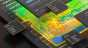
Power distribution issues can silently undermine your PCB’s reliability. This article uncovers the top three failure modes and shows how Power Analyzer by Keysight helps you catch them early in the design phase and how Altium Agile Teams turns those checks into structured team action.

Read More
Embedded thumbnail for Do 90-Degree Bends Destroy Signal Integrity? The Surprising Answer
How-To's • Jan 12, 2026
Do 90-Degree Bends Destroy Signal Integrity? The Surprising Answer

Discover why the long-held belief about 90-degree PCB traces may be more myth than reality. This video explains key signal integrity principles and uncovers insights that can help you make more informed design decisions.

Start Watching
Blog • Dec 11, 2025
From BOM to Requirements and Back: Building Sourcing Constraints Into Specs

When engineering and procurement remain disconnected, supply-chain problems will sneak up on you. This guide argues convincingly: embed sourcing constraints into your requirements from day one, and avoid costly rework down the line.

Read More
Embedded thumbnail for Taking Control Without Adding Complexity – Presentation Embedded World North America 2025
New in Altium Designer 20 • Dec 10, 2025
Taking Control Without Adding Complexity – Presentation Embedded World North America 2025

See how Altium makes project oversight faster and smarter with automated workflows, real-time tracking, and connected design data without adding work for engineers. Watch our Embedded World North America 2025 presentation to learn more.

Start Watching
Blog • Dec 9, 2025
Understanding Power Integrity in PCB Design: Power Analyzer by Keysight Whitepaper

Power integrity is the backbone of reliable PCB design. This whitepaper explains how to analyze and optimize voltage drop, current density, and grounding directly within Altium Designer Agile using the Power Analyzer by Keysight.

Read More
  • Show More
Tag (field_common_tag)
Where to place AC Caps on PCIe Lanes
Blog • Jul 26, 2022
AC Coupling Capacitors in PCIe Routing

Coupling capacitors find plenty of uses in analog applications and on differential protocols, acting essentially as high pass filters that remove DC bias carried seen on a signal. In the case of PCIe, there are a few reasons to place AC coupling capacitors on differential pairs beyond the fact that AC coupling capacitors are listed in the standard. In this article, we’ll look briefly at where to place coupling capacitors on PCIe links, as well as the reasons these are placed on PCIe links.

Read More
Tuning dialog
Blog • Jul 22, 2022
Altium Designer 22.7 Update

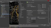
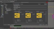
We are happy to announce that the Altium Designer 22.7 update is now available. Altium Designer 22.7 continues to focus on improving the user experience, as well as performance and stability of the software, based on feedback from our users. Check out the key new features in the What's New section on the left side of this window!

Read More
The Positive Impact of Supply Chain Visibility on Design to Cost
Blog • Jul 21, 2022
The Positive Impact of Supply Chain Visibility on Design to Cost

Design to cost is a lofty idea that is only perfectly executed when supply and demand for components are in perfect harmony. Unfortunately, the current landscape for component sourcing makes design to cost more of a balancing act rather than an exercise in price reduction. To help designers in their efforts to balance cost, capabilities, and procurement, we created this ebook to help users understand how modern supply chain tools can help in these complex design problems.

Read More
Evaluating Stubs on PCIe Lanes
Blog • Jul 19, 2022
A Brief Study of Stubs on a PCIe Connector

Stubs are an important topic in high-speed PCB design, and there is a longstanding guideline that stubs should always be removed from all vias on high-speed digital interconnects. While stubs are bad for high-speed lines, they do not always need to be removed. What is more important is to predict the loss profile and frequencies, and to floorplan appropriately to try and prevent such losses.

Read More
Surface Layer DFM and Cleanup
Blog • Jul 14, 2022
PCB Layout Cleanup Before Manufacturing

Once you finish your placement and routing in your PCB layout, it can be tempting to wrap up the layout and send everything in directly to manufacturing. The reality is that the board may still need some work before it is considered finished. The cleanup you perform at the final stage of PCB layout will help you catch any outstanding errors that can't be programmed into your DRC engine, and it gives you a chance to add any outstanding details to the surface layers.

Read More
Low Cost and Professionally Built LED Panel
Blog • Jul 12, 2022
Insulated Metal Substrates: Building an LED Panel

In this project we’ll be building a moderate sized LED panel on insulated metal substrate (IMS). This light panel has three different white balance High CRI LED types on it, warm, neutral and cool. By changing the brightness of the different white balances, the light from the panel can be adjusted to match other lighting, making it perfect for film use - but also creating perfect lighting for electronics work. As with all my projects, this LED panel is open source, you can find the Altium project files over on my GitHub released under the permissive MIT License.

Read More
DFM For Your Materials
Blog • Jul 7, 2022
DFM in PCB Material Selection

Every design should begin with selecting the materials that will appear in the PCB stackup, as well as arranging layers in the stackup to support layout and routing. This section of our PCB manufacturing andc DFM crash course focuses on selecting the right materials for your PCB design. Materials should be selected given the particular design requirements outlined in your specifications.

Read More
PCB Layout for an BGA
Blog • Jul 5, 2022
How to Start an FPGA PCB Layout For Your Embedded System

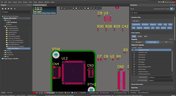
FPGAs come in quad or BGA packages that can be difficult to floorplan, especially with the high number of I/Os often implemented in these components. FPGAs offer a lot of advantages in terms of their reconfigurability, but they can require a lot of effort to layout and route without headaches. If you’ve never worked with an FPGA in your PCB layout, we have some guidelines that can help you get started.

Read More
2-port VNA on a 3-port Network
Blog • Jun 30, 2022
How to Get 3-port S-parameters From a 2-port VNA Measurement

S-parameters are fundamental quantities in signal integrity, and an ability to understand them from measurement or analysis is very important. If you have a 3-port network, like a power divider or circulator, it may appear that you must use a 3-port VNA to measure these S-parameters. It is always acceptable to measure between two ports, but you need to know what exactly it is you are measuring. In this article, we’ll look at the relationship between the true 3-port S-parameters with a 2-port measurement.

Read More
Fab and Assembly Crash Course
Blog • Jun 28, 2022
A Day in the Life of the PCB Manufacturing Process

Before implementing design for manufacturing, it is important to understand the underlying process behind producing a physical PCB. Regardless of the various technologies present in each facility, a large majority of industry-leading manufacturers follow a specific set of steps to turn your design from a drawing in a CAD application into a physical board. In this article, we'll cover the basics that designers need to know as part of our crash course series on PCB manufacturing.

Read More
What Are the Main Skew Sources in a PCB?
Blog • Jun 23, 2022
Addressing Skew Sources in High Speed PCBs

If you compile a list of skew sources, you'll see that fiber weave-induced skew is only one entry on a long list of skew sources. We'll look at this list of possible skew sources below, and we'll see how they affect the operation of your PCB. From the list below, we'll see that some of these issues with skew are not simply solved by paying attention to the fiber weave construction in a PCB substrate.

Read More
Ground Below SMPS Inductors
Blog • Jun 21, 2022
Should Ground Be Placed Below Inductors in Switching Regulators?

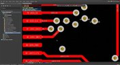
We love answering questions from our readers and YouTube viewers, and one of the recent questions we received relates to EMI from switching elements in a switching regulator is "Should a cutout be placed below the inductor in a switching regulator circuit?". Despite the variations in inductors and their magnetic behavior, there are some general principles that can be used to judge the effects of placing ground near inductors in switching regulator circuits. We’ll look at some of these principles in this article

Read More
Alternative Pins
Blog • Jun 17, 2022
Altium Designer 22.6 Update

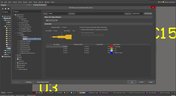
We are happy to announce that the Altium Designer 22.6 update is now available. Altium Designer 22.6 continues to focus on improving the user experience, as well as performance and stability of the software, based on feedback from our users. Check out the key new features in the What's New section on the left side of this window!

Read More
Make PCB Design Reviews Fun Again!
Blog • Jun 16, 2022
Join PCB Design Review Competition from Altium

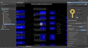
Find 9 mistakes in a PCB design and get added into the lucky draw to win a prize from Altium!

Read More
Top 5 Questions Regarding Stack Up
Blog • Jun 14, 2022
SAP (Semi-Additive PCB Process) – Top 5 Questions Regarding Stack Up

This Semi-Additive Process is an additional tool in the PCB fabricators' toolbox that enables them to provide feature sizes for trace width and spacing that are 25 microns, (1 mil) and below depending on the fabricators' imaging equipment. This provides much more flexibility to breakout out tight BGA areas and the ability to shrink overall circuit size and/ or reduce the number of circuit layers in the design. As the PCB design community embraces the benefits of this new printed circuit board fabrication technique, there are of course many questions to be answered.

Read More
Three ways to manage your BOM costs
Blog • Jun 9, 2022
Improving Supply Chain Success with BOM Management

It’s no secret that component shortages have become more frequent this year. In fact, countries around the world are losing billions in revenue due to supply issues. Having the right components on hand is more crucial than ever as availability, obsolescence, counterfeit products and environmental non-compliance risks continue to grow. Fortunately, many shortages can be avoided by introducing proactive supply chain practices.

Read More
  • Show More
Tag (field_common_tag)
Embedded thumbnail for Searching for Errors
• Jun 16, 2020
Searching for Errors

We’ve looked at how to set up the Design Rule Checker to help us analyze our PCB design errors. Now it’s time to resolve these errors and prep our design to start generating output files.

Start Watching
Embedded thumbnail for Performing Board DRC
• Jun 16, 2020
Performing Board DRC

Design rules are crucial to a PCB’s overall design and performance. It’s just as important to adhere to these rules and ensure that we didn’t overlook any unconnected nets or short circuits. This is why we need to run a Design Rule check.

Start Watching
Embedded thumbnail for Placing a Custom 3D Body in 3D View
• Jun 16, 2020
Placing a Custom 3D Body in 3D View

With the help of the 3D view, it is possible to view a PCB design from all sides, to check on component placement, silkscreen alignment, and many other visual aspects.

Start Watching
Embedded thumbnail for Silkscreen Placement
• Jun 16, 2020
Silkscreen Placement

The silkscreen layer is the layer on which we print any visual text or symbols on our PCB. With the help of this silkscreen layer, we can print our component designators, pin placement, and more.

Start Watching
Embedded thumbnail for Working with Polygon Pours
• Jun 16, 2020
Working with Polygon Pours

When working with common signals, the current levels are usually quite minimal, but when working with power nets it’s not uncommon to see current levels of a few amps. One of the reasons to use polygons is to maintain the quality and reliability of the power supply system.

Start Watching
Embedded thumbnail for Routing Post Processes
• Jun 16, 2020
Routing Post Processes

Depending on how you routed your board, it may be a time-consuming process to fix these manually. So we’ll dive into Route Glossing a little more, along with an automated way to retrace pre-existing routes.

Start Watching
Embedded thumbnail for PCB Layout Cleanup
• Jun 16, 2020
PCB Layout Cleanup

After the board has been routed, it’s almost certain that you’ll need to either move, delete, or adjust some traces. We’ll be looking at a few basic methods to easily modify and remove traces in our design.

Start Watching
Embedded thumbnail for Differential Pair Routing
• Jun 16, 2020
Differential Pair Routing

Routing Differential Pairs is similar to routing single traces, but there are additional rules and guidelines to follow that will help you avoid signal integrity problems.

Start Watching
Embedded thumbnail for Introduction to Routing
• Jun 16, 2020
Introduction to Routing

We’ve looked at different routing behaviors and options that we can change to make routing much easier. So we’re going to dive into the basics of routing and how these settings and routing modes can be applied.

Start Watching
Embedded thumbnail for Defining the Layer Stackup
• Jun 10, 2020
Defining the Layer Stackup

The PCB is designed and formed as a stack of layers and the definition of the PCB layer stack is a critical element of successful printed circuit board design. In Altium Designer, the Layer Stack Manager is used to develop the printed circuit board internal design including layer-pairing, careful via design, any back drilling requirements, rigid/flex requirements, copper balancing, layer stack symmetry, and material compliance. This video guides you through creation of a layer stackup, adding the necessary layers, as well as adding an impedance profile.

Start Watching
Embedded thumbnail for Searching for Errors in Schematic
• May 20, 2020
Searching for Errors in Schematic

Searching for Errors: Errors and mistakes happen to everyone - from beginners to professionals. So we always preach how it is paramount for your design to be validated before pushing it to the PCB. But luckily it’s pretty easy to find and analyze any errors using Altium Designer. We’ll take a look at how to find and analyze errors in your schematic.

Start Watching
Embedded thumbnail for Creating Net Classes
• Jun 2, 2020
Creating Net Classes

A Net Class is a collection of nets that can be used for creating a targeted design rule. So for example, you may want all power and ground nets to have a minimum track width to handle a specific current rating. So we’ll show you how to assign these nets to a NetClass. 

Start Watching
Embedded thumbnail for Configuring Design Rules - Part 2
• May 14, 2020
Configuring Design Rules - Part 2

Altium Designer uses the concept of Design Rules to define the requirements of a design. These rules collectively form an instruction set for the PCB Editor to follow. They cover every aspect of the design - from routing widths, clearances, plane connection styles and so on. With a well-defined set of design rules, you can successfully complete board designs with varying and often stringent design requirements.

Start Watching
Embedded thumbnail for Routing Modes and Setup
• May 12, 2020
Routing Modes and Setup

Most of you know that routing can be a time consuming process, but it doesn’t have to be a daunting task if you have the right tools. So we’ll be looking at what options and settings can help us perfect the art of routing.

Start Watching
Embedded thumbnail for PCB Component Placement
• May 12, 2020
PCB Component Placement

Component placement in the PCB is an important stage of the design process as it sets the precedent for efficient and clean routing. We’ll be diving into different component placement methods along with some tips and tricks that you can use to make this an easy process. 

Start Watching
Embedded thumbnail for Configuring the Basic Rules
• May 12, 2020
Configuring the Basic Rules

Altium Designer uses the concept of Design Rules to define the requirements of a design. These rules collectively form an instruction set for the PCB Editor to follow. They cover every aspect of the design - from routing widths, clearances, plane connection styles and so on. With a well-defined set of design rules, you can successfully complete board designs with varying and often stringent design requirements.

Start Watching
  • Show More
Tag (field_common_tag)
ADv25
On-Demand Webinar • Oct 24, 2024
Modernizing Engineering Workflows: Altium Designer 25 and the Future of Concurrent Design
Struggling with team misalignment and design errors? Join our exciting webinar to discover the groundbreaking advancements in Altium Designer 25!
Watch Now
KiCad Webinar
On-Demand Webinar • Oct 16, 2024
Taking the Next Step: Growing Beyond KiCad with Altium
Join our upcoming webinar to discover how Altium Designer can transition your KiCad projects without any data loss
Watch Now
Synchronize to Optimize Jira Integration
On-Demand Webinar • Oct 7, 2024
Synchronize to Optimize: Enhancing Efficiency with Jira Integration for Altium 365
Tired of juggling multiple tools for project management? Watch the webinar and see how Jira Integration for Altium 365 can optimize your workflows.
Watch Now
Wire bonding
On-Demand Webinar • Sep 29, 2024
Unlock New Design Possibilities with Wire Bonding
Explore how wire bonding can enhance your designs, provide size reduction, improve power management, and increase mechanical reliability.
Watch Now
routing
On-Demand Webinar • Sep 29, 2024
Advanced Routing Features & Techniques
To help you get the most out of your experience with Altium Designer, join our webinar this month and learn advanced routing techniques.
Watch Now
signal analyzer
On-Demand Webinar • Sep 25, 2024
Signal Integrity Made Simple
Discover how to easily detect and resolve high-speed signal integrity challenges without the need for extensive expertise.
Watch Now
competitive-displacement-webinar-3
On-Demand Webinar • Sep 20, 2024
Mastering Design Complexity: How Altium Designer Outperforms Cadence in Solving Workflow and Engineering Challenges - Part 2
Join our webinar to learn how to enhance efficiency, foster better collaboration, and accelerate your time-to-market with Altium unified solutions.
Watch Now
Breaking Down Silos Webinar
On-Demand Webinar • Sep 16, 2024
Breaking Down Data Silos: A Practical Comparison of Altium and Cadence in Cross-Functional PCB Design
Join us for a webinar that addresses the critical challenges of maintaining design data continuity across various design functions.
Watch Now
Draftsman
On-Demand Webinar • Sep 10, 2024
Mastering Design Complexity: How Altium Designer Outperforms Cadence in Solving Workflow and Engineering Challenges
Join our upcoming webinar to discover why engineers consistently choose Altium Designer as the standard in PCB design.
Watch Now
SPICE
On-Demand Webinar • Sep 3, 2024
Mastering SPICE Simulation in Altium Designer
Discover how the SPICE engine in Altium Designer can help you easily verify that your finished project functions as intended.
Watch Now
Output job
On-Demand Webinar • Aug 24, 2024
Beyond PCB Design with Altium Designer
In this webinar we'll dive into the essential aspects that go beyond the schematic and layout.
Watch Now
PCB
On-Demand Webinar • Aug 23, 2024
Elevate Your Design Skills: Tips & Tricks for Success
Discover practical insights and efficient methods that can enhance your PCB design capabilities.
Watch Now
Cyber Security Webinar Cover
On-Demand Webinar • Aug 6, 2024
The Anatomy of IT Compliance in Electronics Development: Altium 365 & AWS GovCloud
Are you an IT or security professional looking for a secure electronics design collaboration platform that could also support your ITAR and EAR compliance efforts? If so, watch this webinar to bring together the expertise of Altium 365 and AWS!
Watch Now
Design reuse
On-Demand Webinar • Aug 1, 2024
How to Speed-up Product Development with Reusable Circuitry
In this webinar you'll learn more about the benefits of the design reuse blocks approach as well as the Design Reuse panel.
Watch Now
Harness design
On-Demand Webinar • Jul 19, 2024
Stay Ahead of the Curve: A Half-Year Review of Altium Designer Improvements
Join our exciting webinar to discover the groundbreaking advancements in Altium Designer!
Watch Now
Lenght Tuning
On-Demand Webinar • Jun 26, 2024
Achieve Precision and Speed with Altium Designer 24's Innovative Routing Features
Speed up your routing process and achieve better results for even your most demanding designs.
Watch Now
  • Show More
Tag (field_common_tag)
Loading
Loading...
Share link
Share with
Search by Update
Version
Update
25 26 24 23 22
25.0 25.1 25.2 25.3 25.4 25.5 25.6 25.7 25.8 25.9
26.1 26.2
24.10 24.9 24.8 24.7 24.6 24.5 24.4 24.3 24.2 24.1 24.0
23.11 23.10 23.9 23.8 23.7 23.6 23.5 23.4 23.3 23.2 23.1 23.0
22.11 22.10 22.9 22.8 22.7 22.6 22.5 22.4 22.3