Results


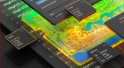
Power distribution issues can silently undermine your PCB’s reliability. This article uncovers the top three failure modes and shows how Power Analyzer by Keysight helps you catch them early in the design phase and how Altium Agile Teams turns those checks into structured team action.


When engineering and procurement remain disconnected, supply-chain problems will sneak up on you. This guide argues convincingly: embed sourcing constraints into your requirements from day one, and avoid costly rework down the line.


Power integrity is the backbone of reliable PCB design. This whitepaper explains how to analyze and optimize voltage drop, current density, and grounding directly within Altium Designer Agile using the Power Analyzer by Keysight.


Strong hardware starts with strong libraries. Discover how disciplined ECAD-library management dramatically improves design consistency and accelerates every stage of your PCB workflow.


Even with all the good guidelines out there for high speed design, there are particular aspects of stackup construction and their relation to building boards that get overlooked. This blog is goes beyond just the typical SI/PI guidelines and looks at these problems from more of an engineering perspective.
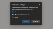
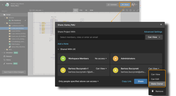
With the latest update to task assignment notifications, project-level and workspace-level tasks will send notifications when events are assigned, or a user is mentioned in a task’s comment. The notifications ensure that people are notified and fully engaged even when they are not actively working on a given project.

Stitching vias are something you often see spread around the surface layer of a PCB, but what are they? and should you be using them? In this guide, we'll go over some of the standard uses of stitching vias and when they should be used in a PCB.
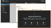
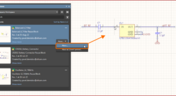
This feature allows you to upload and attach any simulation file to an Altium 365 project. A strict association with the project makes the files easily accessible and traceable for any project collaborators or audit purposes.

In comparison to the build-up of a PCB, the stackup is more concerned with the electrical type of each layer, that is are we working with signals, power, or ground. Continue reading to learn how you can optimize your layer stack.

Transformers used for 50/60 Hz power conversion must be physically larger than those used in wall-warts. Read this article and you will understand why.

Altium’s VP of marketing Lawrence Romine discusses the multi-board and harness design capabilities coming in Altium Designer 23.

Controlled ESR capacitors are important for power integrity in your design as they can help smooth out the PDN impedance spectrum in your high speed PCB.

Due to the great success of the first Altium 365 PCB Competition—in terms of submissions and feedback we received—we partnered with Phil’s Lab for a second edition. This time, we designed a real board that includes some common mistakes. If you find at least one mistake in this PCB design, you can enter a draw to win a $200 gift card!

Whenever we say something to the effect of “components can’t work without a correctly designed PCB,” we only have to look at component packaging for evidence. It is true that component packages come with parasitics that affect signal integrity, but there is one area that we don’t often look at in terms of component packaging: power integrity.
The Assembly App helps reduce the time and increase the accuracy of the manual assembly of printed-circuit boards (prototypes or short runs). Engineers no longer need to flip through paper printouts or navigate CAD software while working on board assembly.

In this article, we’ll look at all that is required to start creating your own custom microcontroller-based hardware designs. You’ll see that there actually isn’t too much to this, as microcontroller manufacturers over the years have tried to make the learning curve less steep and their devices more, and more accessible. This is both from an electrical point of view but also – equally importantly – from a programming point of view.

If you’ve taken time to learn about PCB material options and layer constructions, you have probably seen the wide range of materials that are available on the market. Materials companies produce laminates with varying Dk values, Tg values, weave styles, CTI values, and mechanical properties to target various applications in the electronics industry.