News & Updates


Blog
•
Using ECAD Software to Track Part Availability During PCB Design
As component lead-times extend and obsolescence becomes a persistent threat, PCB projects demand more than schematic capture and layout tools alone. This article details how ECAD software with embedded supply-chain intelligence can: unify engineering and procurement teams; provide visibility into stock levels, lead times and alternates; and enable proactive risk mitigation within the design loop.


Blog
•
PCB Design Data Management Tips for Multi-Board Projects
In complex electronic systems, managing data from multiple printed circuit boards can quickly become a logistical challenge. This article outlines a structured workflow for handling both board-level and assembly-level design outputs, ensuring clarity and consistency across fabrication, assembly and product-level documentation.


Blog
•
6 Areas Your PCB Design Reviews Should Focus On
Learn the six essential topics every electronics team should address in design reviews to improve quality, avoid surprises and bring products to market faster.

Blog
•
What Is BOM Management? A Practical Guide to Avoiding Costly Part Mismatches
From design to production, effective Bill of Materials (BOM) management is critical to ensuring smooth collaboration between engineering, procurement, and manufacturing teams. In this practical guide, we break down proven strategies for structuring, maintaining, and synchronizing your BOM to prevent costly mistakes and accelerate time-to-market.

Blog
•
Requirements Portal Introductory Tutorials
This series of guided demos shows how the Altium Requirements Portal transforms scattered requirement spreadsheets and emails into traceable, version-controlled data that stays aligned with your PCB design efforts.

Blog
•
Bridging the Gap: When to Use Rigid-Flex Instead of Flex & Connector
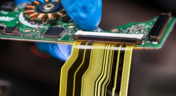
Discover when a rigid-flex PCB is a better choice than a separate flex circuit and connector, especially for designs requiring compact packaging, repeated motion or high reliability. The article emphasizes that although rigid-flex needs more upfront planning and fabrication collaboration, it often pays off in simpler assemblies and improved performance.


Blog
•
Bridging Mechanical and Electrical Teams for Smarter Automotive Design
As vehicles evolve into advanced electronic systems, the separation between electrical and mechanical design teams becomes a critical bottleneck. This article explores how synchronized ECAD–MCAD workflows help automotive projects move faster, reduce rework and maintain design integrity.


Blog
•
Via Structures: Designing for Reliability, Not Just Density
We all want to pack more into our PCB designs, but the smallest via isn’t always the smartest one. Dive in to learn how picking the right structure can save you headaches down the line.


Blog
•
How Structural Electronics Enables 3D, Flexible, and Wearable Integration
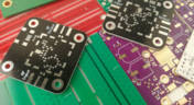
Structural electronics integrates electronic functionality directly into the physical structure of a product, eliminating the need for traditional circuit boards. This article examines how advances in materials, additive manufacturing, and flexible substrates are enabling compact, 3D, and wearable systems with enhanced performance and design freedom.

Blog
•
Beyond Traces: Why Soldermask May Be the Critical Factor in Ultra HDI
In ultra-HDI designs, soldermask is no longer a passive coating but a pivotal element that can determine manufacturability. This article explores why mask registration, resolution, and feature tolerances become critical as line spacings shrink below 50 µm.


Blog
•
How to Use a Multicad Viewer for Seamless Collaboration
Working across different ECAD tools can make design reviews messy and inefficient. This article shows how a multi-CAD viewer simplifies collaboration by letting teams view, comment, and manage designs in one place.
NEW

Blog
•
Breaking the Multiboard Bottleneck: How Unified Design Solves ECAD–MCAD Disconnects
This article examines how fragmented ECAD-MCAD workflows create costly misalignments, late-stage conflicts, and inefficiencies in multiboard system design. It shows how unified, collaborative platforms enable real-time synchronization, digital twins, and cross-domain visibility to eliminate rework and streamline development.

Blog
•
Altium Designer vs. Flux For Professional PCB Projects
Choosing the right PCB tool can define your entire design workflow. Discover how Altium Designer empowers professional product development, while Flux.ai keeps things simple for fast experimentation.
Blog
•
Rigid-Flex Stackups: Where Good Designs Go Wrong Before Layout Even Starts
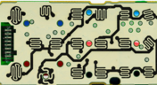
Rigid-flex stackups are more complex than they seem and getting them wrong early can lead to costly failures later. This article shows how smart decisions around materials, transitions, and layer structure help ensure a reliable design.

Blog
•
From Complexity to Clarity: Smart Design Reviews for Agile Engineering Teams
Understand how structured design reviews within Altium Agile Teams enhance visibility, traceability, and cross-team collaboration. This webinar highlights methods to detect issues early and optimize your development workflow.

Blog
•
Building a Local-LLM Datasheet Extractor for IC Driver Development
Parsing long datasheets manually slows down embedded development and introduces errors. This article shows how to use a local LLM pipeline to convert datasheets into structured data that speeds up driver creation.

Blog
•
Types of Simulation Tools For PCBs
PCB simulation isn’t one-size-fits-all and that’s where it gets interesting! Discover the wide range of tools available, from quick circuit checks to advanced multiphysics simulations, and how they help you design with confidence.

Blog
•
Wiring the Future: The Shift to Unified Electromechanical Design
This article explores the shift from PCB-centric design to complex, system-level development where wiring and harnesses play a critical role in product performance. It highlights how unified electromechanical workflows and bi-directional ECAD–MCAD integration improve accuracy, reduce delays, and ensure reliable, production-ready designs.
Blog
•
Best Tools For PCB DFM Checks
Want to catch manufacturability issues before they turn into expensive delays? Discover the essential DFM tools from real-time checks to post-layout analysis that help you get your PCB right the first time.

Blog
•
Eliminate Your Design Friction with Agile Teams
Design friction from scattered data and disconnected tools slows down PCB development and leads to rework. This webinar shows how Agile Teams streamlines collaboration, aligns domains, and helps teams deliver faster with fewer errors.

Blog
•
What Is an Integrated Design Environment for Electronics?
Using multiple disconnected tools slows down PCB development and increases the risk of errors. This article shows how an integrated environment keeps all design data connected, enabling faster workflows and fewer late-stage issues.

Blog
•
What is the Best Cloud PCB Design Software?
Not all cloud PCB tools are created equal, especially when design complexity increases. This article breaks down key differences between cloud-native and hybrid solutions, helping engineers choose the right approach for performance and scalability.

Blog
•
From Rework to Revenue: Digital PCB DFMA
This article explores how traditional, manual DFMA workflows lead to costly rework, delays, and poor collaboration across engineering teams. It shows how a connected, digital approach enables better data integrity, faster design cycles, and improved manufacturing outcomes.

Blog
•
Introducing Octopart Discover: From Part Search to Solutions Discovery
Octopart has announced Octopart Discover, a new platform that shifts electronic component search toward system-level solution discovery. The tool connects design intent with relevant options, enabling engineers to evaluate tradeoffs and identify the best-fit solutions more efficiently.

Blog
•
How to Choose the Right Components for Your BOM
A strong BOM can make the difference between smooth production and costly delays. Discover a practical approach to choosing components that stay available, meet compliance requirements, and keep your project on schedule.

Blog
•
From Scattered Requirements to Confident Product Development
See how the Requirements Portal transforms disconnected requirements into a single, live source of truth that engineers can trust at every stage of a project! Real customer stories in the article prove it’s already helping teams cut down on rework and bring products to market faster.
















Your search returns no results.


