News & Updates

Blog
•
We're heading to PCB West 2025!
Join Altium at PCB West 2025 in Santa Clara, CA, on October 1! Stop by Booth 300 for the official launch of the new Altium platform, built on the foundation of Altium Designer and Altium 365. Be sure to check out our live demos of Altium Develop and Altium Agile.

Blog
•
Peak Electrical Performance in Multi-Board Designs With Advanced Simulation and Compliance Tools
Moving from single-board to multi-board systems is a leap in complexity. You must manage not just routing, but power, signal integrity, mechanical fit, and regulatory requirements across boards. In this article, you’ll discover how Altium’s advanced simulation and compliance tools help engineering teams overcome these challenges and deliver reliable multi-board solutions.

Blog
•
How to Catch Enclosure and Connector Misalignment Before the First Prototype
As electronics continue to miniaturize and functionality increases, even minor misalignments between enclosures and connectors can derail a project. This article explores how early integration of ECAD and MCAD workflows helps detect and eliminate those costly issues before the first prototype is built.
Blog
•
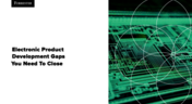
Executive Insights Into Electronic Product Development Gaps You Need To Close
Electronics hardware development is falling behind broader product development disciplines due to fragmented workflows, poor collaboration, and limited compliance visibility. This gap introduces risk, delays, and missed opportunities but executives see real business value in modernizing electronics development through better integration, traceability, and lifecycle visibility.

Blog
•
Sourcing For High-Mix Low-Volume Electronics Manufacturing
High-mix, low-volume (HMLV) electronics manufacturing requires agile sourcing strategies to handle shifting BOMs, erratic lead times, and component volatility. All while controlling costs and ensuring compliance. Cloud-based tools like Altium provide real-time component visibility, BOM collaboration, and supplier integrations to help navigate HMLV complexities.


Blog
•
How to Solve Fit, Form, and Function Challenges in Robotics with ECAD-MCAD Collaboration
As robotics systems become increasingly miniaturized and intricate, ensuring perfect fit, form, and function across electrical and mechanical domains is critical to avoid design setbacks. Real-time ECAD-MCAD integration with two-way sync empowers teams to streamline workflows, reduce PCB rework, and deliver more reliable designs faster.

Blog
•
One Vision, Three Powerful Solutions: Introducing Octopart Discover, Altium Develop, and Altium Agile
We are excited to announce the launch of three new platform-based solutions that will transform the way electronic products are designed, built, and delivered: Octopart Discover, Altium Develop, and Altium Agile. These solutions are designed to simplify processes, accelerate innovation, and make collaboration seamless across the entire electronics lifecycle. Together, they realize the purpose of Altium and Renesas: To Make Our Lives Easier.

Blog
•
The Cost of Overreaction: How Misguided Orders Disrupt the Semiconductor Market
Discover how short-sighted ordering practices fuel volatility in the semiconductor market and why smarter, data-driven approaches are key to building resilience and sustainability.

Blog
•
The Top 5 Workflow Bottlenecks Slowing Down Mechanical Engineering Teams
Mechanical engineering teams frequently encounter delays from fragmented communication, disconnected toolchains, and inefficient synchronization processes. This article examines five critical workflow bottlenecks and highlights how ECAD-MCAD integration with real-time, bidirectional updates can eliminate rework and accelerate design iterations.
Blog
•
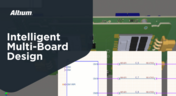
Optimize Your Multiboard PCB System with Intelligent Design and Manufacturing Solutions
Optimizing multiboard PCB systems demands visibility across logical, physical, and manufacturing domains. This article outlines how Altium’s environment lets engineers establish system‑level schematics, 3D spatial validation, harness documentation, and synchronized outputs to streamline design and production.

Blog
•
Why Mechanical Engineers Struggle With ECAD Collaboration (And How to Fix It)
If you’ve ever been frustrated by clunky PCB-to-mechanical workflows, you’re not alone. Learn why collaboration between mechanical and electrical engineers is harder than it should be and what’s behind the struggle.
Blog
•
Digital Thread for Electronics: Synchronizing PCB, Multi-Board, and Harness Design
Eliminate costly mismatches and assembly delays. This whitepaper shows you how to apply a unified digital thread across PCB, multi-board, and harness workflows - bridging ECAD/MCAD silos, ensuring connector accuracy, mechanical fit, and real-time collaboration for flawless system design.

Blog
•
Access to your Training Certificates on My Altium
Introduce an update on the My Altium user page that highlights your certificates and tracks your training progress, with one-click access to the Training Dashboard and Training Catalog pages. Easily view and share your certificates, keep an eye on your learning journey, and explore a variety of training resources.

Blog
•
Rigid-Flex PCBs: Advantages and Challenges
In this article, we will begin with a basic explanation of how rigid-flex technology differs from rigid board technology. We will then provide an overview of the advantages and conclude with a discussion of the challenges to be aware of.
Blog
•
When Should You Use Intrusive Soldering?
Through-hole components are frequently employed in power electronics, particularly when dealing with AC power from a wall outlet. In this article, you can delve into the intrusive soldering process and discover when it can be applied in PCB design.
Blog
•
Unveiling the Crucial Role of PCB Harness Design Capabilities in Multi-Board Designs
Multi-board designs are the key to meeting evolving demands, requiring robust PCB Harness Design for seamless interconnection and success. Join us as we explore the importance of PCB Harness Design capabilities and how they are crucial for the success of multi-board designs.

Blog
•
What Makes a PCB Enclosure Rugged?
Whether you purchase products off-the-shelf or online, they all come housed within an enclosure. In some cases, these enclosures are intentionally ruggedized to withstand harsh environments or mechanical shocks. You can learn more about enclosures in this new and interesting article.
Blog
•
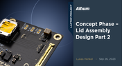
Concept Phase – Lid Assembly Design Part 2
We are continuing our journey through the lid assembly design phase of our Open Source Laptop project. In this section, we will discuss the layout of the test adapter and provide a demonstration of the first test for the display panel, along with the initial steps involved in assembling the boards.
Blog
•
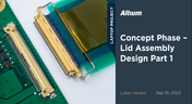
Concept Phase – Lid Assembly Design Part 1
In the exciting next phase of the open-source laptop project we're (finally) diving into design, and getting hands-on with the display panel. Discover how we're selecting the right panel, integrating it seamlessly, and creating a custom DisplayPort adapter to illuminate the screen. Plus, learn how our choices impact features like microphones, webcams, and touch sensors, and how Altium can help bring it all to life. It’s not too late to join as we continue on this innovative journey!
Blog
•
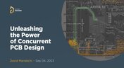
Unleashing the Power of Concurrent PCB Design
Concurrent PCB Design is essential to unlocking the full potential of engineering teams and delivering innovative products that meet the demands of the modern world. Learn more about the main capabilities and the numerous benefits of this upcoming feature in Altium Designer.

Blog
•
Crosstalk Reduction and Elimination Techniques in Altium Designer
Whether you're designing a digital board with a ton of traces, or an RF board operating at very high frequencies, any electronic device with propagating signals will experience crosstalk. Learn more about some sure-fire ways you can reduce crosstalk in your high-speed designs.

Blog
•
Baxandall Volume Control for Audio
The Baxandall volume control is an especially useful, flexible, and simple-to-implement circuit for numerous audio designs. In this article, we will demonstrate how to design this type of equipment.

Blog
•
Common Flex Design Mistakes and How to Fix Them
Designing flexible circuits involves managing numerous factors. Discover how to prevent mistakes in this process and how to rectify them post-implementation.

Blog
•
How Much PCB Mask Expansion is Too Much?
In this article you will learn about finding the right balance between PCB mask expansion and potential problems.
Blog
•
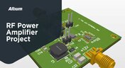
RF Power Amplifier Module PCB Design
RF power amplifiers can be found in many wireless products, often integrated into chipsets or modems. However, in certain specialized systems, you might require higher power output at a specific frequency. This necessitates a discrete amplifier circuit to deliver that power. In this article, we present an example project for a power amplifier that you can incorporate into your RF project.

Blog
•
Avoid GIGO in Your PCB Simulation Tools
Simulation tools are extremely useful for understanding electromagnetic behavior in a design. Learn more about how to avoid obtaining inaccurate results during your PCB simulation process.
Blog
•
Choosing a Converter or Regulator For Your Power Supply Design
When designing the power supply for your device, there are lots of different options. In this article, we will take a brief tour of the main choices in DC power supply design.

Blog
•
The Benefits of Ultra HDI
Learn more about the combination of using both flexible materials and ultra-HDI feature sizes in this article.
















Your search returns no results.


