News & Updates
Blog
•
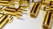
PCB Mountable Connectors: SMD vs. Through-hole
Selecting a connector is as much an art as it is a science. The artistic side is all about aesthetics and satisfying clearances, while the scientific side is all about signal integrity. For PCB mountable connectors, you’ll need to choose between surface-mounted or through-hole connectors, and you’ll need to consider how each type affects signal integrity in your application. Here’s what you need to think about beyond the standard connector specifications.

Blog
•
PCB Via Current-Carrying Capacity: How Hot is Too Hot?
Trace and via current-carrying capacity are legitimate design points to focus on when designing a new board that will carry high current. The goal is to keep conductor temperatures below some appropriate limit, which then helps keep components on the board cool.
Blog
•
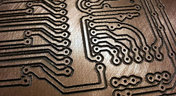
How to Maximize Copper in Your PCB Design: The Pros and Cons of Copper Pouring Versus Placing
There is a saying in copper pour PCB design, “Copper is free.” It means a PCB editor designer must think in reverse. A board starts off as solid copper, and the copper you don’t want is removed. It is faster to build, less consumptive, and less expensive to make a board that is mostly copper as compared to the same size board that is mostly bare. Picking the correct technique will make the difference between an effortless or frustrating experience.


Blog
•
Top 5 PCB Design Guidelines Every PCB Designer Needs to Know
What’s the key to designing a board that’s realistic on paper and in physical form? Let’s explore the top 5 design guidelines that you need to know to design your next manufacturable, functional and reliable PCB.


Blog
•
May 14, 2020
How to Highlight Nets in Altium Designer to Simplify Schematic and PCB Designs
Highlighting nets will help you simplify your schematic and PCB design. In Altium , there are multiple options that enable you to leverage this capability to simplify the verification of connections and circuit paths and make sure that the design you send to your manufacturer accurately reflects the printed circuit board you need built.

Blog
•
May 12, 2020
Keep Your Altium Designer PCB Layout in Line with Grids and Grid-Selection Shortcuts
The grid system in a printed circuit board design CAD system really is your friend, and if you haven’t taken the time to get properly introduced yet let me help you with that.

Blog
•
May 7, 2020
How to Panelize Your PCBs Before Lunch with Altium Designer
Whether you have a slew of PCBs to mass produce for your customers or a handful of project boards you wish to prototype all in one simple swoop, panelization is an effective way to bring high amounts of efficiency to your production.

Blog
•
May 5, 2020
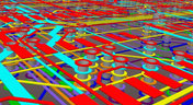
Helpful Tips for Interactive Routing in Altium Designer
Before you jump into the software, you should know the types of things you’re going to want to look out for. Traces, connection lines, differential pair routing, and route paths can all affect the routing process of your board. Make sure that you’re equipped knowing, ultimately, what you want your board design to accomplish and furthermore, where you anticipate potential problem areas to be.

Blog
•
May 1, 2020
Altium 365 + Altium Designer 20.1 Released Today - Work from Anywhere, Connect with Anyone
In our efforts to bring the best experience to the PCB design process, we are proud to announce the release of Altium Designer 20.1, Altium 365, and Altium NEXUS Client 3.1. This release enhances the design experience by bringing the convenience and benefits of the Altium 365 cloud platform to Altium Designer.


Blog
•
Apr 27, 2020
Introduction to High Speed PCB Designing: How to Eliminate Crosstalk
Crosstalk on your PCB layout can be disastrous. If not corrected, crosstalk can cause your finished circuit board to either not work at all, or it may be plagued by intermittent problems. Let’s take a look at what crosstalk is and what you can do to prevent it.


Blog
•
Apr 22, 2020
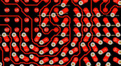
Any Angle Routing: When Should You Use It?
EDA tools have come a long way since the advent of personal computing. Now advanced routing features like auto-routers, interactive routing, length tuning, and pin-swapping are helping designers stay productive, especially as device and trace densities increase. Read full article in our blog:


Blog
•
Mar 20, 2020
A Message from Altium on COVID-19
We understand that many of you, like ourselves, have transitioned to working remotely. This process comes with its challenges and we would like to offer all and any help we can to minimize disruptions for your teams and business.

Blog
•
Bridging Mechanical and Electrical Teams for Smarter Automotive Design
As vehicles evolve into advanced electronic systems, the separation between electrical and mechanical design teams becomes a critical bottleneck. This article explores how synchronized ECAD–MCAD workflows help automotive projects move faster, reduce rework and maintain design integrity.
Blog
•
Via Structures: Designing for Reliability, Not Just Density
We all want to pack more into our PCB designs, but the smallest via isn’t always the smartest one. Dive in to learn how picking the right structure can save you headaches down the line.

Blog
•
How Structural Electronics Enables 3D, Flexible, and Wearable Integration
Structural electronics integrates electronic functionality directly into the physical structure of a product, eliminating the need for traditional circuit boards. This article examines how advances in materials, additive manufacturing, and flexible substrates are enabling compact, 3D, and wearable systems with enhanced performance and design freedom.
Blog
•
Beyond Traces: Why Soldermask May Be the Critical Factor in Ultra HDI
In ultra-HDI designs, soldermask is no longer a passive coating but a pivotal element that can determine manufacturability. This article explores why mask registration, resolution, and feature tolerances become critical as line spacings shrink below 50 µm.

Blog
•
How ECAD-MCAD Co-Design Supports Aerospace Reliability and Compliance
When the margin for error is nearly zero, aerospace engineering demands a design process that’s seamless across all domains. Here, we explore how ECAD-MCAD co-design delivers an integrated workflow that supports first-pass success and compliance with strict aerospace standards.

Blog
•
Most Common Causes of PCB Assembly Rework and Scrap
Many PCB assemblies fail not because of exotic faults, but due to basic issues like incorrect BOM entries or footprint mismatches that force rework or scrap. This article dives into the most common causes and how to prevent costly defects in your design-to-manufacturing process.

Blog
•
Behind the Scenes with AI Embedded Development
Forget one-shot AI hacks Ari Mahpour shows the thoughtful, sustainable way to integrate AI into embedded firmware development. Learn the core principles (planning gate, HAL abstraction, observability, timeout design) that can help you push your efficiency 5-10 times in real hardware projects.

Blog
•
We're heading to PCB West 2025!
Join Altium at PCB West 2025 in Santa Clara, CA, on October 1! Stop by Booth 300 for the official launch of the new Altium platform, built on the foundation of Altium Designer and Altium 365. Be sure to check out our live demos of Altium Develop and Altium Agile.

Blog
•
Peak Electrical Performance in Multi-Board Designs With Advanced Simulation and Compliance Tools
Moving from single-board to multi-board systems is a leap in complexity. You must manage not just routing, but power, signal integrity, mechanical fit, and regulatory requirements across boards. In this article, you’ll discover how Altium’s advanced simulation and compliance tools help engineering teams overcome these challenges and deliver reliable multi-board solutions.

Blog
•
How to Catch Enclosure and Connector Misalignment Before the First Prototype
As electronics continue to miniaturize and functionality increases, even minor misalignments between enclosures and connectors can derail a project. This article explores how early integration of ECAD and MCAD workflows helps detect and eliminate those costly issues before the first prototype is built.

Blog
•
Executive Insights Into Electronic Product Development Gaps You Need To Close
Electronics hardware development is falling behind broader product development disciplines due to fragmented workflows, poor collaboration, and limited compliance visibility. This gap introduces risk, delays, and missed opportunities but executives see real business value in modernizing electronics development through better integration, traceability, and lifecycle visibility.

Blog
•
Sourcing For High-Mix Low-Volume Electronics Manufacturing
High-mix, low-volume (HMLV) electronics manufacturing requires agile sourcing strategies to handle shifting BOMs, erratic lead times, and component volatility. All while controlling costs and ensuring compliance. Cloud-based tools like Altium provide real-time component visibility, BOM collaboration, and supplier integrations to help navigate HMLV complexities.

Blog
•
How to Solve Fit, Form, and Function Challenges in Robotics with ECAD-MCAD Collaboration
As robotics systems become increasingly miniaturized and intricate, ensuring perfect fit, form, and function across electrical and mechanical domains is critical to avoid design setbacks. Real-time ECAD-MCAD integration with two-way sync empowers teams to streamline workflows, reduce PCB rework, and deliver more reliable designs faster.
Blog
•
One Vision, Three Powerful Solutions: Introducing Octopart Discover, Altium Develop, and Altium Agile
We are excited to announce the launch of three new platform-based solutions that will transform the way electronic products are designed, built, and delivered: Octopart Discover, Altium Develop, and Altium Agile. These solutions are designed to simplify processes, accelerate innovation, and make collaboration seamless across the entire electronics lifecycle. Together, they realize the purpose of Altium and Renesas: To Make Our Lives Easier.

Blog
•
The Cost of Overreaction: How Misguided Orders Disrupt the Semiconductor Market
Discover how short-sighted ordering practices fuel volatility in the semiconductor market and why smarter, data-driven approaches are key to building resilience and sustainability.

Blog
•
The Top 5 Workflow Bottlenecks Slowing Down Mechanical Engineering Teams
Mechanical engineering teams frequently encounter delays from fragmented communication, disconnected toolchains, and inefficient synchronization processes. This article examines five critical workflow bottlenecks and highlights how ECAD-MCAD integration with real-time, bidirectional updates can eliminate rework and accelerate design iterations.
















Your search returns no results.


