Welcome, Guest

Sign in to learn, create, and do more with the product you love.

News & Updates

Filters:
Tag
Embedded thumbnail for Clearly Show Jumper Wires in Your Harness Designs
New in Altium's Software
Clearly Show Jumper Wires in Your Harness Designs

Support has been improved so that jumper wires connecting two cavities within the same connector are now properly shown in Layout Drawings, making the connector wiring easier to understand during documentation and review.

Blog
From Scattered Requirements to Confident Product Development

See how the Requirements Portal transforms disconnected requirements into a single, live source of truth that engineers can trust at every stage of a project! Real customer stories in the article prove it’s already helping teams cut down on rework and bring products to market faster.

Embedded thumbnail for Why Datasheet PCB Guidelines Are Often Wrong
How-To's
Why Datasheet PCB Guidelines Are Often Wrong

Watch our brand-new video where we tackle the persistent issue of outdated PCB design guidelines still found in datasheets and application notes from major semiconductor manufacturers. Drawing on viewer comments, real-world datasheet examples, and insights from industry experts, we examine why recommendations such as splitting analog and digital ground planes (an approach rooted in the 1980s) continue to circulate despite their potential to cause EMC failures, signal integrity problems, and costly redesigns.

Blog
What is the Best PCB Design Tool For Students?

Students need PCB software that’s intuitive, affordable, and useful for building real skills. This article compares the strengths and weaknesses of leading design tools, from hobbyist platforms to industry-standard software.

Embedded thumbnail for Keep Your Harness Designs in Sync with Library Updates
New in Altium's Software
Keep Your Harness Designs in Sync with Library Updates

The "Update From Libraries" feature has been enhanced to provide broader support for harness-related objects across both Wiring Diagrams and Layout Drawings. With this expansion, a wider range of harness components such as connectors, wires, splices, and associated attributes can now be synchronized directly with their corresponding library definitions.

Blog
What Is Collaborative Engineering?

Collaborative engineering is all about breaking down silos so electrical, mechanical, and sourcing teams can work as one with shared data and real-time updates. This article shows how that approach helps you spot issues early, reduce rework, and get products out the door with fewer surprises.

Embedded thumbnail for How to Set Up Flex PCB Materials in Altium
How-To's
How to Set Up Flex PCB Materials in Altium

Discover how to set up flex and rigid-flex PCB materials in Altium with the Layer Stack Manager. In this tutorial, you’ll follow the key steps for defining polyimide cores, adhesive layers, coverlay, and stiffeners helping you build accurate, production-ready rigid-flex PCB designs.

Blog
Bend Reliability: How Trace Geometry and Materials Impact Flex Lifespan

Focused on durability under repeated mechanical stress, this piece details how routing strategy, copper thickness, adhesive systems, and bend radius selection determine flex lifespan. Engineers will find actionable recommendations for reducing strain concentration and improving long-term performance in high-cycle applications.


Embedded thumbnail for How Benchmark Unifies Hardware Development with the Altium Platform
Altium Stories
How Benchmark Unifies Hardware Development with the Altium Platform

Discover our latest customer success story and see how Benchmark streamlined hardware development using the Altium Platform. By leveraging a unified environment with real-time data, synchronized ECAD-MCAD workflows, and built-in collaboration tools, their engineering teams eliminated manual handoffs, improved cross-domain visibility, and accelerated project delivery while staying perfectly aligned.

Blog
PCB Design Process: The EDA Design Approach

Dive into how a modern EDA workflow transforms PCB design by linking electrical, mechanical, and manufacturing requirements from idea to final release. With constraint‑driven integration, you can cut down on respins and bring better boards to market faster.
Embedded thumbnail for ESP32-S3 Design Deep Dive: Power, RF, and Layout Best Practices
How-To's
ESP32-S3 Design Deep Dive: Power, RF, and Layout Best Practices

Explore our detailed design review of a custom ESP32-S3 PCB. This four-layer board is built around the ESP32-S3 microcontroller chip (not the standard module) and includes an integrated LiPo charging circuit, USB-C with data line protection, NCP voltage regulators, and a ceramic chip antenna with a properly tuned impedance matching network.

Blog
Getting Started for Mechanical Engineers

Explore our collection of MCAD Collaboration walkthroughs, where you’ll discover how to synchronize mechanical constraints and keepouts, maintain traceability with advanced history and revision control, and streamline electromechanical connectivity through harness synchronization. These topics and many more are covered in this article.


Embedded thumbnail for Working as One for What Matters Most | How Benchmark Unifies Engineering Teams
Altium Stories
Working as One for What Matters Most | How Benchmark Unifies Engineering Teams

See how Benchmark Electronics uses Altium’s collaborative hardware development platform to unify its electrical, mechanical, and software engineering teams. By replacing manual processes, disconnected tools, and siloed workflows with a shared workspace, Benchmark unlocked a new way of working.

Blog
Are Your ECAD Tools Holding Back Engineers’ Productivity?

The article highlights that productivity issues often stem from tool limitations rather than engineer effort, especially as project complexity grows. ECAD tools that offer clear version control, cross-discipline integration, and workflow awareness are key to sustaining efficiency.

Embedded thumbnail for PCB Design Tips to Improve RF Power Amplifier Layout
How-To's
PCB Design Tips to Improve RF Power Amplifier Layout

Take a deeper look at RF power amplifier PCB design as we expand on our original 6 GHz RF signal generator tutorial with an in-depth design review. Discover essential layout optimization techniques such as switching regulator routing, feedback loop placement, stitching via implementation, and effective copper balancing.

Embedded thumbnail for How Altium's Assembly Assistant unifies Quantum Systems' Dev Process
Altium Stories
How Altium's Assembly Assistant unifies Quantum Systems' Dev Process

Quantum Systems develops unmanned drone systems for aerial intelligence and rapid, field-ready innovation. With the Assembly Assistant, their team streamlined a once tedious prototype build process, eliminating manual exports, file conversions, and unnecessary guesswork.

Embedded thumbnail for Creating Stacking Stripes for PCB Fabrication: Altium Tutorial
How-To's
Creating Stacking Stripes for PCB Fabrication: Altium Tutorial

Watch our new tutorial where we demonstrate how to place stacking stripes along the edge of a PCB and configure design rules to control clearances. In this video, you’ll learn how to create a dummy net, use the query system to apply rules specifically to stacking stripes, and leverage split planes on internal layers.

Tag
Blog
Additive PCB Manufacturing: The Vaccine for Electronics Supply Shocks?

At this time, at least a quarter of the world’s population is under quarantine, with workers unable to go to offices or factories, leading to fundamental disabling of the world economy. The electronics industry is suffering greatly as well, dealing with a supply shock from factories shutting down in Southeast Asia, to demand-side shocks from Western markets literally shutting down. Now it is the electrical engineers taking the lead with additive PCB manufacturing.
Article preview
Blog
Webinar "6 Steps to Master Project Storage"

Altium 365 provides a secure cloud platform to store all of your design files in a single place so you can share them with anyone and access them from anywhere. This webinar discusses the advantages of placing, storing, and working with projects in Altium 365.

Article preview
Blog
Altium Designer 20 Changed My Layout Design Routines

I just finalized my first PCB design using Altium Designer 20. At the same time, I tested some new AD20 features, and in this article, I’ll share my thoughts about new layout design features which made the biggest impression for me: sliding, and any-angle routing.

Article preview
Blog
Designing for Antenna Isolation in Your Wireless System

Anyone who has taken apart an old cell phone or designs IoT devices knows multiple communication capabilities are present in these designs, each requiring different antennas. The RF designer should already take precautions for interconnect isolation, but antenna isolation is just as important when modeling and designing wireless systems.

Blog
PCB Trace and Pad Clearance: Low vs. High Voltage

High voltage/high current designs carry safety requirements which need to be met by designers. Similarly, high speed designs need to have suppressed crosstalk in order to ensure signal integrity. The key design aspects that relate to both areas are your PCB trace clearance and pad clearance values. These design choices are critical for balancing safety, noise suppression, and manufacturability.

Blog
Getting Through PCB DFM

In this article, we’ll discuss the key design features to implement, and steps to take prior to fabrication that will help prevent some DFM process pain.
Altium Designer Getting Started User Guide
Blog
Level Up Your Design Skills - Altium Designer Getting Started User Guide Update
We are happy to announce the new update of our Altium Designer Getting Started User Guide. Whether you are new to Altium Designer or you want to brush up on some topics, the Altium Designer Getting Started User Guide will take you from a beginner to a master in PCB design.  This is only the beginning! This guide will be updated with new information based on user feedback. Let’s first go over the contents of the guide.

Article preview
Blog
Modeling Copper Foil Roughness in Altium Designer's Impedance Profiler

With the new layer stack manager in Altium Designer®, you can now include copper foil roughness factors directly in your impedance calculator. This is quite easy to do in the layer stack manager, but it begs the question: what exactly is the copper roughness factor? Which value should be used for your interconnects?

Article preview
Blog
High-Speed Signal Routing: The 5 Important Constraints

After you capture your schematic as an initial layout and create an initial component arrangement, it’s time to define your routing constraints. Doing this early will allow your DRC engine to spot rules violations before you finish your layout. Likewise, you’ll be able to modify the default rule set to meet your layout requirements. Here are the important routing constraints you’ll need to check before you start routing your board.
Blog
How to Create a PCB Manufacturing Cost Estimation

Some manufacturers have very convenient PCB manufacturing cost estimation calculators you can use, but the real costs depend on a number of factors. If you’re an entrepreneur and you’re producing your own boards, or you are managing manufacturing, testing, and delivery for a new project, it’s your job to help clients understand the primary cost drivers for new boards. Here’s how you can get an estimate of your fabrication costs, both for local and overseas manufacturers.
Blog
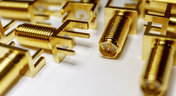
PCB Mountable Connectors: SMD vs. Through-hole

Selecting a connector is as much an art as it is a science. The artistic side is all about aesthetics and satisfying clearances, while the scientific side is all about signal integrity. For PCB mountable connectors, you’ll need to choose between surface-mounted or through-hole connectors, and you’ll need to consider how each type affects signal integrity in your application. Here’s what you need to think about beyond the standard connector specifications.

Article preview
Blog
PCB Via Current-Carrying Capacity: How Hot is Too Hot?

Trace and via current-carrying capacity are legitimate design points to focus on when designing a new board that will carry high current. The goal is to keep conductor temperatures below some appropriate limit, which then helps keep components on the board cool.
Blog
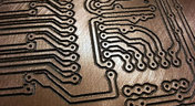
How to Maximize Copper in Your PCB Design: The Pros and Cons of Copper Pouring Versus Placing

There is a saying in copper pour PCB design, “Copper is free.” It means a PCB editor designer must think in reverse. A board starts off as solid copper, and the copper you don’t want is removed. It is faster to build, less consumptive, and less expensive to make a board that is mostly copper as compared to the same size board that is mostly bare. Picking the correct technique will make the difference between an effortless or frustrating experience.

Article preview
Blog May 14, 2020
How to Highlight Nets in Altium Designer to Simplify Schematic and PCB Designs

Highlighting nets will help you simplify your schematic and PCB design. In Altium , there are multiple options that enable you to leverage this capability to simplify the verification of connections and circuit paths and make sure that the design you send to your manufacturer accurately reflects the printed circuit board you need built.


Tag
NEW
Embedded thumbnail for  Improve Visual Accuracy with True Arcs
New in Altium's Software
Improve Visual Accuracy with True Arcs

Discover how True Arc Rendering improves arc visualization in the PCB Editor and PCB Library Editor by displaying true arcs across 2D, 3D, and Board Planning modes. This provides a more accurate representation of board geometry and helps you work with curved features with greater precision throughout the design process.

NEW
Embedded thumbnail for Two engineers, one board, nobody's work gets wiped out
Collaborative Engineering with Team Ribbot
Two engineers, one board, nobody's work gets wiped out

When Team Ribbot’s electrical and mechanical engineers work on the same combat-robot design, unwanted changes can mean hours of lost work. See how Altium Designer and MCAD CoDesign let the team review and selectively accept changes, enabling seamless parallel collaboration across different locations and schedules.

Embedded thumbnail for Visualize and Refine Your Harness Designs
New in Altium's Software
Visualize and Refine Your Harness Designs

Create detailed views of bundle contents, control wire and cable paths, and rotate physical models to accurately represent the final harness assembly. These capabilities give you greater control over harness design and help ensure your digital model reflects the physical result.

Embedded thumbnail for Introducing Agentic Requirements Engineering
New in Altium's Software
Introducing Agentic Requirements Engineering

Discover a new way to work with Requirements Portal through Agentic Requirements Engineering. AI agents analyze your project data and surface proposals for your approval, reducing friction in requirements management and helping align your team's shared model with your design intent.

Embedded thumbnail for Simplify Rule Set Updates and Replacement
New in Altium's Software
Simplify Rule Set Updates and Replacement

Learn how to import rule sets with greater flexibility in Altium. When importing rules, you can add new rules to your existing set, replace only rules that match, or completely replace the current rule set giving you full control over how design rules are updated.

Embedded thumbnail for  How Team Ribbot fits 40 kW of power into a 250-pound combat robot
Collaborative Engineering with Team Ribbot
How Team Ribbot fits 40 kW of power into a 250-pound combat robot

What do you get when you pack the power of a small electric car into a combat robot with virtually no room to spare? In the first episode of our collaboration with Team Ribbot and Altium, explore how seamless ECAD-MCAD collaboration helps the team tackle complex design challenges, optimize high-performance designs, reduce errors, and bring products to life faster.

Embedded thumbnail for Just Released: Supplier Data Merging
New in Altium's Software
Just Released: Supplier Data Merging

Discover how the Supplier Data Merging feature brings together supplier information from your custom parts database and the Altium Parts Provider into a single, unified view. Access consolidated supplier data wherever supplier part numbers appear, including in ActiveBOM and during component selection.

Embedded thumbnail for How Altium’s Layer Stack Manager Actually Works
How-To's
How Altium’s Layer Stack Manager Actually Works

Take a look inside Altium's Layer Stack Manager and discover how its impedance calculator determines the ideal trace width for your target impedance. In this video, we break down the "black box" behind the calculation and show how the Simbeor-based field solver provides accurate results while eliminating the need for advanced field solver expertise.

Embedded thumbnail for Connect Requirements Directly to Your PCB Design
New in Altium's Software
Connect Requirements Directly to Your PCB Design

See how the Requirements Portal integration in Altium Designer simplifies requirements management by bringing system requirements directly into your PCB design workflow. Connect requirements to design documents, assign tasks, track verification in real time, and keep your entire team aligned with seamless synchronization in Altium 365.

Embedded thumbnail for SFP Connector Routing: High-Speed Differential Pair Design Tips
How-To's
SFP Connector Routing: High-Speed Differential Pair Design Tips

Discover practical SFP and SFP+ routing tips in our latest video, inspired by a real question from the Altium subreddit. We cover how aggressive serpentine length tuning can be, how to reduce impedance discontinuities in tight meanders, and how meandering influences mode conversion at 10G and higher data rates.

Embedded thumbnail for Handle High-Density PCB Layouts with Ease
New in Altium's Software
Handle High-Density PCB Layouts with Ease

Push the limits of PCB design with support for up to 128 signal layers, empowering the development of even the most complex, high-density boards.

Embedded thumbnail for Skip Layer Routing for RF: Control Impedance & Cut Insertion Loss
How-To's
Skip Layer Routing for RF: Control Impedance & Cut Insertion Loss

Discover our latest video and learn how RF designers use a deeper ground plane to minimize skin-effect resistance, improve signal integrity over long high-frequency routes, and optimize impedance matching for oversized SMT pads in antenna launches and coaxial connectors.

Embedded thumbnail for Just Released: ODB++ Intellectual Property Protection
New in Altium's Software
Just Released: ODB++ Intellectual Property Protection

ODB++ Intellectual Property Protection lets you control exactly what design data is included in the ODB++ output, ensuring each manufacturing partner receives only the information needed for their specific fabrication or assembly tasks.

Embedded thumbnail for Future of Electronics Development in Security and Aerospace
How-To's
Future of Electronics Development in Security and Aerospace

See the highlights from Altium's executive event in Hamburg, where Security and Aerospace leaders explored AI-driven development, digital engineering, supply chain resilience, and the future of mission-critical electronics.

Embedded thumbnail for Create Clearance Rules Faster and with Less Effort
New in Altium's Software
Create Clearance Rules Faster and with Less Effort

Setting up clearance rules is now more intuitive in the Constraint Manager. Choose the Simple view for faster configuration with grouped object types, or the Advanced view when you need detailed, matrix-based clearance control.

Embedded thumbnail for Mastering HDI Design Rules in Altium Designer
How-To's
Mastering HDI Design Rules in Altium Designer

In our latest Altium Academy tutorial, we guide you through configuring the essential HDI PCB design rules in Altium's software. You'll learn how to use your manufacturer's fabrication capabilities to create accurate design rules and constraints for your PCB.

Tag
Your search returns no results.