News & Updates
Blog
•
Registration Challenges in UHDI: Why Fabrication Tolerances Matter in Your Layout
As UHDI structures shrink, achieving accurate layer-to-layer registration becomes less forgiving than ever. Learn why fabrication tolerances matter so much in ultra-fine geometries and how to design with registration limits in mind from the start.

Blog
•
How Engineering Project Management Tools Are Changing Engineering Teams’ Productivity
Engineering project management tools play a critical role in managing timelines, resources, and cross-disciplinary coordination. This article breaks down the most impactful systems for improving execution and team performance.

Blog
•
7 Ways to Catch Rules & Constraints Early – Checklist
Discover seven actionable ways to spot and fix rules and constraint issues before they derail your PCB project. Using Altium Designer Agile, these tips help you build more manufacturable and reliable boards with fewer iterations.
Blog
•
Do You Need an IPC-D-356 Netlist?
If your output package is Gerber-based, adding an IPC-D-356 netlist can dramatically improve how your design is reviewed and validated for production. Here’s when it matters, what it contains, and how to generate it quickly in Altium.


Blog
•
How Agile BOM Management Helps You Lock in Pricing Before Market Shifts
When engineering and procurement work from different BOM versions, delays and cost surprises follow. Learn how agile BOM management brings teams onto one connected BOM so they can respond fast, manage risk, and lock pricing early.


Blog
•
Flexible Circuits: Enhancing Performance with Shielding, Heat Dissipation, and Stiffeners
A flex circuit can look perfect on paper and still fail in the real world due to EMI, hot spots, or mechanical strain. This article breaks down how shielding, thermal planning, and stiffeners help deliver designs that stay reliable over time.

Blog
•
Avoid These Top 3 Power Distribution Failures in PCB Design
Power distribution issues can silently undermine your PCB’s reliability. This article uncovers the top three failure modes and shows how Power Analyzer by Keysight helps you catch them early in the design phase and how Altium Agile Teams turns those checks into structured team action.


Blog
•
From BOM to Requirements and Back: Building Sourcing Constraints Into Specs
When engineering and procurement remain disconnected, supply-chain problems will sneak up on you. This guide argues convincingly: embed sourcing constraints into your requirements from day one, and avoid costly rework down the line.

Blog
•
Understanding Power Integrity in PCB Design: Power Analyzer by Keysight Whitepaper
Power integrity is the backbone of reliable PCB design. This whitepaper explains how to analyze and optimize voltage drop, current density, and grounding directly within Altium Designer Agile using the Power Analyzer by Keysight.

Blog
•
How to Manage ECAD Libraries for Consistent PCB Layout Design
Strong hardware starts with strong libraries. Discover how disciplined ECAD-library management dramatically improves design consistency and accelerates every stage of your PCB workflow.

Blog
•
Properties panel document options in SCH editors
The Properties panel provides access to the properties of documents and objects. The contents of the panel change depending on the active document or the selected object. This blog will quickly go over some of need to know options around the properties panel in the schematic document.
Blog
•
The High-Speed PCB Stackup Design Challenge
Even with all the good guidelines out there for high speed design, there are particular aspects of stackup construction and their relation to building boards that get overlooked. This blog is goes beyond just the typical SI/PI guidelines and looks at these problems from more of an engineering perspective.
Blog
•
Everything You Need to Know About Stitching Vias
Stitching vias are something you often see spread around the surface layer of a PCB, but what are they? and should you be using them? In this guide, we'll go over some of the standard uses of stitching vias and when they should be used in a PCB.
Blog
•
PCB Stackup Basics
In comparison to the build-up of a PCB, the stackup is more concerned with the electrical type of each layer, that is are we working with signals, power, or ground. Continue reading to learn how you can optimize your layer stack.
Blog
•
Multi-board and Harness Design Capability in Altium Designer 23
Altium’s VP of marketing Lawrence Romine discusses the multi-board and harness design capabilities coming in Altium Designer 23.

Blog
•
Controlled ESR Capacitors: Should You Use Them for Power Integrity?
Controlled ESR capacitors are important for power integrity in your design as they can help smooth out the PDN impedance spectrum in your high speed PCB.

Blog
•
How Does the Package PDN Impact Power Integrity?
Whenever we say something to the effect of “components can’t work without a correctly designed PCB,” we only have to look at component packaging for evidence. It is true that component packages come with parasitics that affect signal integrity, but there is one area that we don’t often look at in terms of component packaging: power integrity.
Blog
•
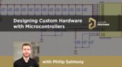
Designing Custom Hardware with Microcontrollers
In this article, we’ll look at all that is required to start creating your own custom microcontroller-based hardware designs. You’ll see that there actually isn’t too much to this, as microcontroller manufacturers over the years have tried to make the learning curve less steep and their devices more, and more accessible. This is both from an electrical point of view but also – equally importantly – from a programming point of view.
Blog
•
Guide to Low-Dk PCB Materials
If you’ve taken time to learn about PCB material options and layer constructions, you have probably seen the wide range of materials that are available on the market. Materials companies produce laminates with varying Dk values, Tg values, weave styles, CTI values, and mechanical properties to target various applications in the electronics industry.

Blog
•
Designing for V2X Communication: Wireless Protocols and Standards
If you’re waiting for truly connected cars on a grand scale, there is still a massive amount of work to be done, both on the hardware and software sides. Connected cars can only become a widespread reality once the automotive industry and telecom carriers can decide which protocol will work best for vehicle-to-everything (V2X) communication. PCB designers will then need to step in to create these systems and fit them into a vehicular environment.
Blog
•
Everything You Need to Know About Stitching Vias
This one area of PCB design can be contentious among some designers as it is related to copper pour, which it is often stated is not needed in most designs. Regardless of your feelings about copper pour, stitching vias have important uses in PCBs at low frequencies and at high frequencies.

Blog
•
IPC-2221 Calculator for PCB Trace Current and Heating
The IPC-2221 standard includes many requirements for printed circuit board design and manufacturability, and there are several online calculators that have been developed based on this standard.
Blog
•
All About Box Build Assemblies
When you’re ready to manufacture a new device at production volume, there are many aspects of the product that must come together. The enclosure, cabling and connectors, embedded software/firmware, and of course the PCBA all have to be considered in totality. There is a quick way to get your product into a usable enclosure, complete with input power and cabling, and with a form factor that fits your PCBA. This overused route to a new product is a box build assembly.
Blog
•
Ultra-HDI Technology is Not New
Printed circuit board fabricators have become skilled at manufacturing these technologies and also at understanding the reliability and producibility challenges associated with high-density-interconnect technology. Let’s look at where the PCB industry is at today.

Blog
•
Today's PCB Designers Are Driving Electronics Product Design
What can the industry do to support PCB designers as they continue taking a more active role in product development? Here at Altium, there has been a progressive shift towards looking at the system level and creating tools that get designers more involved throughout the product development process. As the saying goes, over the wall engineering is over… today’s most successful products are built in a collaborative process.

Blog
•
Phased Array Antenna Design for 5G Applications
As the 5G rollout progresses and researchers continue to discuss 6G, many new 5G-capable products operating in sub-GHz and mmWave bands are reaching the marketplace. Devices that will include a 5G-compatible front-end, whether small stations/repeaters or handheld devices, use phased arrays as high-gain antenna systems to provide high data throughput without losing range at higher frequencies.
















Your search returns no results.


