News & Updates

Blog
•
Using an LDO vs. Switching Regulator in Your PCB
As much as we’d like, the power we supply to electronics isn’t always stable. Real power sources contain noise, they might exhibit power instability, or they dropout unexpectedly. Thankfully, we have power regulators to help prevent some of these problems. For low power devices, we generally see two types of power regulators: a low dropout regulator (LDO) or a switching regulator. You can mix and match these at different points along your power bus, but there’s still the matter of choosing whether to use an LDO vs. a switching regulator in your designs.

Blog
•
Using Altium 365 for Sharing Simulations in the Cloud
Post-layout simulators for your PCB are very valuable tools. If you’re working through a complex design, it’s a good idea to put it through some level of simulation and analysis to evaluate the design before manufacturing. This is all easy with the cloud collaboration tools in Altium 365 and Ansys field solvers thanks to the EDB Exporter utility in Altium Designer. These existing tools in Altium Designer and any of the Ansys field solver utilities give you a simplified way to share design data, EDB files, and simulation results with anyone on your design team.

Blog
•
How to Speed Up Your DFM Report Process in the Cloud
Experienced fabricators will tell you: any design could have some hidden DFM problem that will interfere with manufacturability, quality, or yield. Making use of your design rules is just the start of preventing DFM problems, you’ll want to collaborate with your manufacturer throughout the design process if you want to spot and correct DFM problems. Within Altium Designer, there are multiple reports you can generate for your projects that will help you summarize important information on your board for a client or a manufacturer.

Blog
•
The Digital Engineer's Guide to RF PCB Layout and Routing
With modern systems running at higher frequencies, incorporating multiple wireless protocols, and interfacing with many analog sensors, advanced designs require knowledge from digital and RF design disciplines. If you’re now starting to work in the RF realm and you need to design an all-analog or mixed-signal system, RF PCB layout will need to become a new specialty. If you’re a digital designer and you’re now jumping into high-frequency analog design, keep reading to learn more about RF PCB layout and routing.

Blog
•
Microstrip Ground Clearance: How Close is Too Close?
If you take a look at any guidelines for controlled impedance traces, you’ll clearly see that the trace width is calculated without any ground pour near the trace. However, most designers will state that unused areas on each PCB layer should be filled in with grounded copper pour. If you bring some ground pour near a microstrip, you’ve now formed a coplanar waveguide arrangement. So now the question becomes, how much microstrip to ground clearance do you need to ensure you’ve hit your impedance goals?

Blog
•
PCB Layout Guidelines for Switching Power Supplies and Regulators
In this article, I want to briefly focus on how power supplies and regulators are different, although this should already be clear to most designers. For a power supply and for a PCB with an on-board regulator, the switching regulator layout will be a major determinant of overall system performance. Therefore, we’ll largely look at some layout guidelines for switching power supplies in terms of regulator layout.

Blog
•
PCB Sharing and What Data You Can Share in Altium 365
Altium 365 is giving design teams a new way to share and manage their design data. Most users are probably aware of project-level and component-level PCB sharing features, but sharing actually extends down to the level of individual files thanks to the managed content system within Altium 365. If you’ve ever wanted a single place to store and manage all of your design data, then Altium 365 is here to help you and your team stay organized.

Blog
•
How to Combat Power Supply EMI in Your PCB
Power supplies are one of those systems we all tend to take for granted. Everyone’s first task in power supply design is usually to ensure the voltage and current output reach the desired level, probably followed by thermal considerations. However, due to safety issues, EMC requirements, the use of higher PWM frequencies, and the need for smaller packaging, power supply EMI should be a major design consideration. With that being said, what are the major sources of power supply EMI, and how can power supply designers keep them in check?

Blog
•
Leveraging the Free Footprint Community to Design at Lightning Speed
Designing footprints is a job most people hate. It’s tedious, time-consuming, and doesn’t result in much except, well, a footprint. Companies now realize this pain point and offering designers free, well-designed PCB footprints. Why would they spend their time doing this? In this article, we’re going to review some of the free offerings that exist within the PCB design community. Once you’re armed with this information, you will spend most of your time designing and routing boards instead of pulling your hair out creating footprints all day.

Blog
•
Designing for Multiple PCBs in the Same Project
The majority of our PCB designs sit as a single PCB under our Altium Designer projects. It sometimes happens that we have a single project that requires multiple PCBs with various stuffing options, but when it happens, a lot of us tend to get stuck. How do you handle the exact change across both projects? How do you guarantee those changes to be identical? This article will review an approach to managing multiple PCB designs within a single project, ensuring your single source of truth.

Blog
•
Designing 5G Devices
The next stage in the evolution of mobile telephony is here with the roll-out of 5G. The designer looking to incorporate functionality to handle 5G signals into their circuits will face some challenging issues. So, what’s so special about 5G?

Blog
•
All About Your PCB Trace Length: How Long is Too Long?
The maximum PCB trace length you can place between two components depends on multiple factors, such as signaling protocol, component specification, losses in PCB laminate, and skew. With all this in mind, let’s look at where losses accumulate along the channel.

Blog
•
Using an LDO vs. Switching Regulator in Your PCB
For low power devices, we generally see two types of power regulators: a low dropout regulator (LDO) or a switching regulator. You can mix and match these at different points along your power bus, but there’s still the matter of choosing whether to use an LDO vs. a switching regulator in your designs. If you’ve ever wondered how these decisions are made and when to use each type of regulator, just know that there is more to this decision than simply looking at the input/output voltage/current.

Blog
•
What They Don’t Teach You About Fluxes
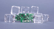
PCB fabrication is an extremely complex technological topic that deserves recognition as the most fundamental part of PCB engineering. Unless connectors, conductive adhesive, wire-bonding, or zebra-tape are used, in the modern electronics industry it’s always necessary to use some kind of flux during the soldering process to create an electric connection. In this article, we’ll discuss fluxes — what they are, what they are made of (yes, there is going to be a lot of chemistry, don’t be scared), how they should be used, and in what direction the industry is going.
Blog
•
Thermal Management for Integrated Circuits
As anyone who designs and builds electronic devices knows, the device will generate heat when it’s switched on. Wherever current flows through an impedance, energy losses will manifest themselves as heat. Integrated circuit packaging is getting smaller to meet the trend for more compact devices but at the cost of poorer thermal properties. This article describes the basic thermal management approaches to consider in your next designs.


Blog
•
Anatomy of Latitude Part Two: "Thread with a Needle” in the context of energy
We continue to explore the magic of energy conversion in a PWM transducer. Why is it magic? Theoretically, in a PWM transducer this happens without losses, isn't that magic? A PWM transducer, like a tailor with scissors, cuts the “fabric of energy” into pieces, and then, like a sewing machine, stitches the pieces of energy into a dress - DC Magnitude. What is a constant component and how can we get it? Let's explore!

Blog
•
Anatomy of Latitude Part One: Pulse Width Modulation (PWM) as a Result of the Evolution of Linear Systems
There are different techniques in the world of technology to achieve various goals, both final and intermediate. Some techniques are so successful that they are commonly used with high efficiency. Electronics is no exception. The greatest example is the use of Pulse Width Modulation (PWM) signals (energy), which is applied in any modern electronic device. To apply PWM effectively, it is necessary to understand the engineering difficulties that engineers faced in the past, and the thoughts and ideas that subsequently were combined into effective, complete PWM power solutions.


Blog
•
What Influences Electrolytic Capacitor Lifespan?
If you speak with a bunch of design engineers, you might quickly form the opinion that the electrolytic capacitor has a particularly dubious reputation. A faulty electrolyte mix used in these types of capacitors led to premature device failures, and quite often, a “bit of a mess” was made to the PCBs on which they were soldered. However, despite the problem of the capacitor plague, this article is focusing on helping the designer understand how to get many more years of useful life from an electrolytic capacitor.

Blog
•
What You Can Track in Your Altium Project History
When you’re working through a new PCB design project, and you need to keep track of your project revisions, Altium 365™ creates the ideal environment for collaborative PCB design and revision tracking. Once you upload your projects onto the cloud through the Altium 365 platform, Altium 365 creates a Git repository for your project. It allows you to make it available to collaborators through Altium Designer®. This includes a complete project history, which can be easily accessed by collaborators working on a complex project.

Blog
•
Gerber Compare in Altium 365's Online Platform
The moment you push your Gerbers to a manufacturer for a DFM inspection, it can be a nerve-wracking experience waiting for a response. Before you receive your working boards, there will likely be some back-and-forth communication before your board hits the fabrication line. When manufacturers and designers need to resolve problems in Gerber files before fabrication, it helps to have a Gerber compare utility. The newest version of Altium Designer now offers this feature through the Altium 365 platform, giving everyone visibility into changes to Gerbers before fabrication.

Blog
•
California Bets on Electric Cars and Plans to Ban Gasoline Car Sales by 2035
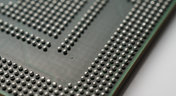
No matter how you might feel about renewable energy and associated environmental issues, electric vehicles are becoming more mainstream and will become the primary mode of transportation in the future. For the engineering community, what’s much more interesting is how our power distribution and management infrastructure can support this shift to massive increases in the use of electricity on the grid. So what’s the rub for PCB designers?
Blog
•
My Favorite Altium Designer Keyboard Shortcuts and Viewing Features
When you’re working through a complex PCB layout, it always helps to know the shortcuts you can use to stay productive. Altium Designer® keyboard shortcuts, and keyboard + mouse shortcuts, can help you easily walk through your PCB layout during design and as part of final checks during a design review. Here are some of my favorite keyboard shortcuts and viewing options that help me stay productive, and I hope they can do the same for you.

Blog
•
The IEEE P370 Standard for High Speed PCB Interconnects
High speed PCB interconnects have continued to remain an active challenge in modeling and simulation, particularly when dealing with broadband signals. The IEEE P370 standard is a step towards addressing the challenges faced by many designers in determining broadband S-parameters for high speed structures up to 50 GHz. Although this standard has been in the works since 2015, it finally passed board approval and appears as an active draft standard.

Blog
•
Class-D Amplifier Design and PCB Layout
Amplifiers can come in all shapes and sizes, depending on their bandwidth, power consumption, and many other factors. A Class-D amplifier design is normally used with high fidelity audio systems, and circuits for a Class-D amplifier are not too difficult to build in a schematic. If you’ve never worked with a Class-D amplifier or you’re looking for a fun audio project, follow along with this PCB layout.

Blog
•
DDR5 vs. DDR6: Here's What to Expect in RAM Modules
Modern digital systems throw the digital electronics textbooks out the window, and high-speed DDR memories are a perfect example of the paradigm shift that occurs when you jump into IC and PCB design. With DDR5 still being finalized, and DDR6 now being discussed, designers who are already comfortable with DDR4 will need to consider how their design practices should adjust to accommodate the constant doubling of data speeds in these high-speed memory technologies.
Blog
•
Making the Most of Your Crystal Oscillator
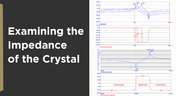
In my experience, the somewhat vague information you might find in a typical crystal datasheet doesn’t enable an engineer to be wholly confident that their design expectations can be met. On the other hand, “blindly” adopting what the crystal datasheet says usually results in adequate frequency stability. If you want to get inside and uncover what is going on, you need to start thinking about the crystal as a phase-shifting network.
Blog
•
How Antipads Affect Signal Integrity in Your Multilayer PCB
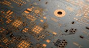
Antipads on vias and landing pads are a point of contention in modern PCB design, and the debate around the use of these elements in a multilayer PCB is framed as a binary choice. Like thermal reliefs, ground plane splits, and orthogonal routing, the debate around antipads on landing pads and vias is framed as an always/never choice. With today’s modern PCBs, it pays to understand the effects of antipads on signal integrity.
Blog
•
How to Design a Microstrip to Waveguide Transition
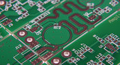
RF structures can be complicated to design and layout, particularly because many RF systems lead double lives as digital systems. Getting an analog signal out of a component and into a waveguide for high isolation routing is not so simple as placing a microstrip or stripline coming off your source component. Instead, you need to create a special microstrip to waveguide transition structure to ensure strong coupling into and out of your waveguide.

Blog
•
Managing PCB Polygon Pour and Copper Features in Complex Layouts
Layouts for complex electrical systems may need to make extensive use of copper pour to provide ground nets, power nets, shielding, and other copper structures for power and signal integrity. Backplanes, motherboards, RF products, and many other complex layouts will make use of copper pour and polygons that can’t be easily placed as custom components. The rules-driven design engine in Altium Designer® also ensures that any PCB polygon pour you place in your PCB layout will comply with clearance rules and will be checked against other electrical design rules.
Blog
•
High Speed Backplane Design and PCB Layout Tips
If you need to connect multiple boards into a larger system and provide interconnections between them, you’ll likely use a backplane to arrange these boards. Backplanes are advanced boards that borrow some elements from high speed design, mechanical design, high voltage/high current design, and even RF design. They carry their own set of standards that go beyond the reliability requirements in IPC.
Blog
•
PCIe 5.0 Signal Integrity and Analysis
The upcoming Gen6 version of PCIe is pushing the limits of signal integrity for many computer systems designers. As with any high-speed signaling standard, signal integrity is a major design consideration, which requires the right set of design and analysis techniques. Rather than digging deep to find PCIe 5.0 signal integrity requirements from PCI-SIG, we’ve compiled the important points for today’s PCB layout engineers. Layout engineers should pay attention here as these design requirements will become more stringent in later PCIe generations.

Blog
•
Top 4 Time Wasters in PCB Design Collaboration
An essential aspect of project management is time management, especially when your design team is working remotely. Your time management strategy is team-based and individual, but time can easily get spent on important tasks when working as part of a team. So how can you streamline important collaboration tasks for your design team to increase productivity?

Blog
•
Sharing Inside and Outside Your Altium 365 Workspace
In these days of easily-available internet and quarantines, everyone is working remotely. It’s nice being able to spend time with family and regain control over your schedule, but keeping track of projects and revisions while securing user access feels like its own job. With the right set of project and data management tools, you can easily share your data with collaborators without tracking email chains.
Blog
•
How Your Altium 365 Workspace Keeps You Organized
When I started using my Altium 365 Workspace for collaboration, I found I could make things run more smoothly when I kept things organized. However, I prevented any issues thanks to all the organization tools built into the Explorer panel within Altium Designer. Let’s take a look at how you can get the most value out of your Altium 365 Workspace in terms of organization and access management.
















Your search returns no results.


