News & Updates


Blog
•
Microstrip Ground Clearance Part 2: How Clearance Affects Losses
If your goal is to hit a target impedance, and you’re worried about how nearby pour might affect impedance, you can get closer than the limits set by the 3W rule. But what are the effects on losses? If the reason for this question isn’t obvious, or if you’re not up-to-date on the finer points of transmission line design, then keep reading to see how nearby ground pour can affect losses in impedance-controlled interconnects.

Blog
•
Choosing the Right Microphone for Embedded Applications
If you need to capture sound waves for your electrical device to process, you'll need a microphone. However, microphones these days have become very advanced, and there are so many options to choose from. They range from the relatively simple and popular condenser type microphones to state-of-the-art sound conversion solutions incorporating internal amplifiers and other electronic processing functionality. In this article, we'll take a look at some of the options available.


Blog
•
Composite Amplifiers and How They Give the Best of Both Worlds
There are many times where you need an amplifier with high gain, low noise, high slew rate, and broad bandwidth simultaneously. However, not all of these design goals are possible with all off-the-shelf components. Here are some points to consider when working with a composite amplifier design and how to evaluate your design with the right set of circuit simulation tools.

Blog
•
Reduce Common-Mode Noise in Your Power Supply with Impedance Balancing
Simple switching regulator circuits that operate in compact spaces, like on a small PCB, can usually be deployed in noisy environments without superimposing significant noise on the output power level. As long as you lay out the board properly, you’ll probably only need a simple filter circuit to remove EMI on the inputs and outputs. As the regulator becomes larger, both physically and electrically, noise problems can become much more apparent, namely radiated EMI and conducted EMI in the PCB layout.


Blog
•
Part 1: Why Your PCB Design Review Process Is Obsolete and What You Can Do About It
A PCB design review is a practice to review the design of a board for possible errors and issues at various stages of product development. It can range from a formal checklist with official sign-offs to a more free-form inspection of schematic drawings and PCB layouts. For this article, we will not delve into what to check during a design review process but rather look at how a review process itself usually unfolds and how to optimize it to get the most out of your time.

Blog
•
Part 2: Why Your PCB Design Review Process Is Obsolete and What You Can Do About It
As we established in Part 1, the PCB design review and collaboration practices have room for improvement in many organizations. To address this, we developed Altium 365. Let's examine how running a PCB project through Altium 365 compares to other methods.


Blog
•
What is PCB Star Grounding and Why Would Anyone Use It?
If you look on the internet, you'll find some interesting grounding recommendations, and sometimes terminology gets thrown around and applied to a PCB without the proper context or understanding of real electrical behavior. DC recommendations get applied to AC, low current gets applied to high current, and vice versa... the list goes on. One of the more interesting grounding techniques you'll see as a recommendation, including on some popular engineering blogs within the industry, is the use of PCB star grounding.

Blog
•
Your Guide to PCB Silkscreen
Every PCB has silkscreen on the surface layer, and you’ll see a range of alphanumeric codes, numbers, markings, and logos on PCB silkscreen. What exactly does it all mean, and what specifically should you include in your silkscreen layer? All designs are different, but there are some common pieces of information that will appear in any silkscreen in order to aid assembly, testing, debug, and traceability


Blog
•
What Causes Gibbs Ringing in High-speed Channel Simulations?
Designing high-speed channels on complex boards requires simulations, measurements on test boards, or both to ensure the design operates as you intend. Gibbs ringing is one of these effects that can occur when calculating a channel’s response using band-limited network parameters. Just as is the case in measurements, Gibbs ringing can occur in channel simulations due to the fact that network parameters are typically band-limited.

Blog
•
Efficient Heat Dissipation with SMD Heat Sinks Keeps You From Dropping PCBs
In electronics, there is the possibility that your PCB can get pretty hot due to power dissipation in certain components. There are many things to consider when dealing with heat in your board, and it starts with determining power dissipation in your design during schematic capture. If you happen to be operating within safe limits in a high power device, you might need an SMD heat sink on certain components. Ultimately, this could save your components, your product, and even the operator.


Blog
•
RF Power Supply Design and Layout Guide
One thing is certain: power supply designs can get much more complex than simply routing DC power lines to your components. RF power supply designs require special care to ensure they will function without transferring excessive noise between portions of the system, something that is made more difficult due to the high power levels involved. In addition to careful layout, circuitry needs to be designed such that the system provides highly efficient power conversion and delivery to each subsection of the system.

Blog
•
Methods to Protect your Circuit
Overvoltage, overcurrent, and heat are the three most likely events that can destroy our expensive silicon-based components or reduce our product’s life expectancy. The effects are often quite instant, but our product might survive several months of chronic overstress before giving up the ghost in some cases. Without adequate protection, our circuit can be vulnerable to damage, so what should we do? Or do we need to do anything?
Blog
•
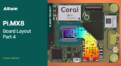
Pi.MX8 Project - Board Layout Part 4
We invite you to explore a new chapter in the PiMX8 Project, focusing on the final stages of PCB layout design for the Pi.MX8 compute module. This installment covers critical topics such as routing power planes and signal delay tuning, essential for ensuring proper functionality and performance.
Blog
•
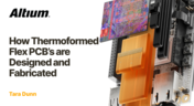
How Thermoformed Flex PCB’s are Designed and Fabricated
Thermoformed flexible PCBs are specially designed and fabricated by heating and molding them into specific shapes, making them suitable for compact and complex applications like automotive dashboards and wearable devices. This process involves precise temperature control and careful handling to ensure durability and quality. Discover more from Tara Dunn's new article.
Blog
•
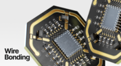
Boost Connection Integrity and Design Efficiency with Wire Bonding
Altium Designer's wire bonding feature enhances PCB design by supporting chip-up configurations for Chip on Board (CoB) designs. It offers easy validation of bond wiring in 3D views, ensuring accurate and efficient design processes. Check more about this feature on Altium's new feature page.
Blog
•
How High Frequency SMD Passives Work in a PCB Layout
High-frequency surface-mount device (SMD) passives like resistors and capacitors play a crucial role in PCB layouts, particularly in circuits operating above 1 GHz. Our article explores how these components function at high frequencies, their operational limits, and the importance of considering parasitic elements in design.

Blog
•
Essential DFM Tips for Aerospace Projects
Design for Manufacturing (DFM) is a crucial aspect of aerospace projects. This process ensures high-quality designs that meet the unique challenges of the aerospace industry, such as extreme conditions and stringent reliability standards. Learn more about essential DFM tips in our brand-new article.

Blog
•
Mechanics Meet Electronics Seamlessly in Multi-Board PCB Design
Curious about the intersection of mechanical and electrical design? Both are crucial in the PCB design process, especially for multi-board systems. Read our latest article to learn how ECAD and MCAD can address significant challenges during PCB preparation.

Blog
•
Altium 365 now has its own website!
Discover everything you need to know about Altium 365 and experience our suite of applications for secure, seamless, and streamlined collaboration. Visit now to explore how to streamline your electronic product development.
Blog
•
Efficient DC-DC Converter Design: Automated Measurements with Altium Designer 24 MixedSim
Automated measurements are no longer tough. With our Mixed Simulation mode, everything is easier. Learn more about this feature based on DC-DC buck converter design in this brand new article.
Blog
•
Altium Designer: Leading the Charge in PCB Design Innovation
In the dynamic field of electronics design, Altium Designer stands out as a pioneer, continuously advancing the boundaries of PCB (Printed Circuit Board) design. Discover the latest innovations in 3D-MID design, high-speed design, and interactive routing in this new article by David Marrakchi.
Blog
•
What Is Solder Mask Expansion and Which Value Should You Use?
Check out our new article explaining how to ensure sufficient pad area for soldering, manage misregistration tolerance, and maintain proper solder dams between components. It also highlights the role of collaboration with fabrication houses and the use of CAD tools in defining land patterns for advanced electronics designs.
Blog
•
Pi.MX8 Project - Board Layout Part 3
We continue our exploration of the Pi.MX8 open-source computer module project. In this new installment, we focus on routing planning and then cover all the layers' routing with all the details you need to know if you want to prepare a similar project.

Blog
•
Mastering Blind and Buried Vias
Check our compilation of essential resources you'll need to use blind and buried vias successfully in an HDI PCB. In our brand new article, we present the main and most valuable information about this technology, which may not be new but is still highly useful in High-Density Interconnect projects.

Blog
•
Penn Electric Racing Pushes the Envelope with Altium 365
Discover how Penn Electric Racing builds award-winning, fully electric racecars with Altium 365, pushing the boundaries of technology and design.
Blog
•
Make Sure to Clean Your No-Clean Flux
No-clean flux has become popular due to its convenience. Learn more about why this solution is used, why cleaning might still be necessary, and how to remove no-clean flux residues. We will try to dispel all these doubts in this brand new article.

Blog
•
SPICE Simulation Module: How To Use Automated Measurements in Simulations To Save Time and Money in Design Challenges
Simulation of electronic circuits is a key factor in the success of your design. A SPICE circuit simulator may be used to speed up the design analysis. Learn more about how Altium Designer can help you with automated measurements, saving you time and money during the design process.
Blog
•
Achieve Seamless Rigid-Flex Design with Altium Designer's Unified Solution
Check out our refreshed feature page about Rigid-Flex PCB Design and see how Altium Designer’s unified environment can help you manage this kind of project with no limitations or additional licensing required.
















Your search returns no results.


