Welcome, Guest

Sign in to learn, create, and do more with the product you love.

News & Updates

Filters:
Tag
Component Management
On-Demand Webinar
Help Ensure The Best Designs With Component Management

There are many aspects to designing a PCB. One of the larger aspects has to do with managing your components. We all need components for our designs, but are those components in our library and designs up-to-date or even purchasable? These questions need to be answered before we can safely use them. If not, we could just be wasting our time designing with invalid components. Altium Designer® has several tools to help you manage the components in your libraries and designs.

Altium Designer Interface
Blog
Altium Designer 22.5 Update

We are happy to announce that the Altium Designer 22.5 update is now available. Altium Designer 22.5 continues to focus on improving the user experience, as well as performance and stability of the software, based on feedback from our users. Check out the key new features in the What's New section on the left side of this window!

Are Hybrid PCB Stackups Reliable?
Blog
How Reliable is Your Hybrid PCB Stackup?

PCB stackups often incorporate slightly dissimilar materials that could pose a reliability problem. Hybrid PCBs are one case where the PCB stackup will include different materials, typically a standard FR4 laminate and a PTFE laminate for RF PCBs. Designers who want to take the lead on material selection when designing their hybrid stackups should consider these factors that affect reliability. As with any PCB stackup, make sure you get your fabricator involved in the manufacturing process early to ensure reliability problems do not arise during production.

Embedded thumbnail for How to Draw a Board Outline Using Coordinates
How-To's
How to Draw a Board Outline Using Coordinates

In this video, we cover how to draw a curve by using coordinates. This can be very helpful when creating a board outline.

Embedded thumbnail for Creating a Schematic Symbol: Mapping out the Component
How to create a Schematic Symbol
Creating a Schematic Symbol: Mapping out the Component

When creating a schematic symbol, one of your first tasks will be creating a component symbol. We’ll show you how to map out a component in the Schematic Library Editor by creating and configuring the component, adding pins, and creating graphics.

Monte Carlo vs Sensitivity Analysis
Blog
Monte Carlo Simulation vs. Sensitivity Analysis: What’s the Difference?

In a previous article about circuit simulation and reliability, I looked at how Monte Carlo analysis is commonly used to evaluate circuits that are subject to random variations in component values. Sensitivity analysis is a bit different and it tells you how the operating characteristics of your circuit change in a specific direction. Compared to a Monte Carlo simulation, sensitivity analysis gives you a convenient way to predict exactly how the operating characteristics will change if you were to deliberately increase or decrease the value of a component.

Embedded thumbnail for How and When to Use Rooms
How to work with Rooms
How and When to Use Rooms

Rooms are an extremely valuable tool within the Altium Designer PCB environment, but how and when do you use rooms? If you need to control component placement and layout, assign a specific design rule to a group of items, or if you have repeated channels that need similar layouts in your multichannel design, rooms can make it much easier.

Simulation, Build and Test
Blog
Creating Continuous Integration Pipelines for FPGAs

Field Programmable Gate Arrays, or FPGAs, have become ubiquitous amongst high-speed, real-time digital systems. The speed at which FPGAs operate continues to increase at a dizzying pace but their adoption into Continuous Integration pipelines seems not to trail as closely. In this article we will review the concept of CI pipelines, their application to FPGAs, and look at examples on how to set this up.

Embedded thumbnail for MCAD CoDesigner Quick Start: Autodesk Fusion 360
Working with MCAD CoDesigner extension
MCAD CoDesigner Quick Start: Autodesk Fusion 360

MCAD CoDesigner is built to address the challenges of electronic product design by enabling seamless collaboration between your electrical and mechanical engineers. This video will show you how to start collaborate between Altium Designer and Autodesk Fusion 360. 

Embedded thumbnail for Component Placement Control for DFM
DFM and Fabrication Cost/Time Constraints
Component Placement Control for DFM

Component placement is a crucial part of making sure your design is manufacturable, so you need to be able to control placement. We’ll show you how, through rules and courtyard layers to maintain accessibility and manufacturability in your entire design through component placement control.

Collaborators Visualization
Blog
Soft Locks [Conflict Prevention] in Altium 365

Conflicts can occur when multiple people work on the same project simultaneously. The user might not realize that they are not looking at the latest version of the documentation, leading to problems later. To address this issue, Altium features an intuitive graphical user interface that allows you to examine conflicts quickly and carefully

Component Creation
On-Demand Webinar
Increase Productivity With Easy Component Creation

Component creation is a necessary evil when it comes to design, and it’s something we all need to do. But instead of spending hours creating your components and having them turn into a complete roadblock, let it be just a simple bump on the road. Altium Designer has several tools available to you in order to create the different aspects of a component, including the symbol, footprint, 3D model parametric data, supply chain information, and more

Guide to Monte Carlo in SPICE
Blog
The Basics of Monte Carlo in SPICE: Theory and Demo

Anytime you place a component in your PCB, it’s almost like you’re gambling. All components have tolerances, and some of these are very precise, but others components can have very wide tolerances on their nominal values. In the event the tolerances on these components become too large, how can you predict how these tolerances will affect your circuits?

Embedded thumbnail for MCAD CoDesigner Quick Start: PTC Creo
Working with MCAD CoDesigner extension
MCAD CoDesigner Quick Start: PTC Creo

MCAD CoDesigner is built to address the challenges of electronic product design by enabling seamless collaboration between your electrical and mechanical engineers. This video will show you how to start collaborate between Altium Designer and PTC Creo

Embedded thumbnail for Variants in Multi-Channel Designs
How to work with Variants
Variants in Multi-Channel Designs

Multi-channel designs can utilize variations in the channels to reduce design time and sheet count. We’ll show you how to take advantage of this by configuring several types of components.

BGA Land Patterns and Footprints
Blog
What's In Your BGA Land Pattern and Footprint

If you look in datasheets for most components, you’ll often find a recommended land pattern, usually alongside some mechanical package information and assembly information. This is not always the case with BGA components, especially components with high ball count. There are a few reasons for this that we can speculate: those ball counts might just be too big to put into a single page, or the manufacturer just expects you to know how to create that land pattern.

Embedded thumbnail for Stackup Considerations
DFM and Fabrication Cost/Time Constraints
Stackup Considerations

There is a lot to consider about the Layer Stackup when it comes to designing a manufacturable board. We’ll walk you through enabling symmetry, finding correct balance of your layers, materials, creating and loading templates, and adding a layer stack table for better communication between you and your manufacturer.

Molded Interconnect Devices
Blog
MIDs Make a Comeback as Vertical SMD Modules for Your PCB

Molded interconnect devices are essentially plastic molded substrates with traces running along any surface, including at right angles and running vertically. Altium users can use the new 3D Routing extension to design their own component carriers, which can be mounted vertically in a standard assembly process. If you’ve always wanted to vertically mount components or entire circuits, but without the expense of adding a flex section to your design, the new 3D Routing extension with HARTING’s component carrier designs provides a unique solution.

Embedded thumbnail for What Are Design Variants For?
How to work with Variants
What Are Design Variants For?

Variants in Altium Designer allow you to create several variations of the same design all from one source project. Variants can be managed in the project and through Altium Designer you can control variants in the PCB, Schematic, Draftsman, and Outjob files to make your designs easily editable without redundancy.

MCAD CoDesign Process
Blog
MCAD CoDesigner 2.9.0 is Out

Altium has released version 2.9.0 of the MCAD CoDesigner. This version has the option to exclude small components when transferring from ECAD to MCAD. The arc behavior was improved, and the support for splines in board shape and cutouts was added. With this release, you can now select a specific SOLIDWORKS configuration of a part to use on the board and view the improvements made for Siemens NX.

Tag
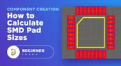
How to Calculate SMD Pad Sizes?
Blog
Best Methods for Calculating SMD Pad Size in PCB Design

SMD components require precisely sized pads for soldering during assembly. The designer is responsible for ensuring pad sizes are correct, either by calculating them and comparing with footprint data, looking through datasheets, or by memorizing SMD pad size standards. If you have a component and you don't have access to the footprint, and you decide to biuld the footprint yourself, what resources are available to ensure you have the correct pad size?

Can You Fix a Warped PCB?
Blog
Can You Fix a Warped PCB?

Before we get too deep into this article, I’ll give you the simple answer. You probably can’t fix warping in your PCB after it’s already been fabricated. You can prevent an unwarped board from becoming warped during assembly, but only as long as materials were selected properly and the board is put into reflow correctly. We’ll run over some of these points in this article, and I’ll examine some points that might help you recover a warped board.

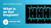
What is an Eye Diagram?
Blog
What is an Eye Diagram?

The eye diagram is a useful measurement or simulation as part of channel compliance. The measurement shows many different factors that can affect signal behavior simultaneously, ultimately allowing for qualification of errors and losses in a channel. In this article, I’ll run over some of the fundamental measurements that you could manually extract from an eye diagram and how they reveal some strategies for improving channel designs.

Skills for Today's PCB Designers
Blog
What Skills Are Needed to be a PCB Layout Designer?

To readers who have been working in the PCB industry for most of your career, you have probably seen a very diverse group of professionals with varied skill sets and backgrounds. Designers might get started as engineers or as technicians, and some designers learn how to create beautiful PCB layouts in university. No matter how you got into PCB design, there are some important skills to know that will take you a long way towards advancing your career.

How to Fix the Top PCB Design Mistakes
Blog
Beginner PCB Design Mistakes and How To Avoid Them

When starting out with PCB design, it’s common to treat the process as simply ‘connecting the dots’: as long as connections are made, it’s not particularly important how these connections are made. Having reviewed quite a number of PCBs of other PCB design engineers over the last few years, there are common, unfortunately erroneous, occurrences between a lot of them. This article aims to illustrate the top five beginner PCB design mistakes and what we can do to avoid making them. Let’s get started!

Top 5 Questions Regarding Stack Up
Blog
SAP (Semi-Additive PCB Process) – Top 5 Questions Regarding Stack Up

As the PCB design community embraces the benefits of this new printed circuit board fabrication technique, there are of course many questions to be answered.  Today’s blog will address some of the most commonly asked questions related to circuit layer stack up as people are introduced to this new technology.

Design Reuse Blocks Update
Blog
Altium Designer 22.9 Update

We are happy to announce that the Altium Designer 22.9 update is now available. Altium Designer 22.9 continues to focus on improving the user experience, as well as performance and stability of the software, based on feedback from our users. Check out the key new features in the What's New section on the left side of this window!

Dual Rail Voltage Supply
Blog
Dual Rail Voltage Supply

The highest performing operational amplifiers often need a split supply with positive and negative voltages connected to the op amps supply rails. In this project, we’re going to be building a positive/negative dual rail power supply for a differential oscilloscope probe I’m designing. I’m making the power supply a separate project, as a dual rail supply is quite useful to have, and I’m sure I’ll find multiple uses for it in the future.

Library Importer Interface
Blog
Library Importer Improvements (former Library Migrator)

Importing file-based libraries from your local computer or network drive to your Altium 365 workspace can be done using the Library Importer. Altium’s Library Migrator was renamed Library Importer—the feature’s name was changed to conform more closely to the tool’s purpose. Not only is its name new, but our team has also made several user experience improvements. We have updated the documentation to reflect this change.

Blog
How to Select Copper Foil for High-Frequency PCB Design

The PCB materials industry has spent significant amounts of time developing materials that provide lowest possible signal loss for products with RF applications. For high speed and high frequency designs, losses will limit signal propagation distance and distort signals, and it will create an impedance deviation that can be seen in TDR measurements. In this article, we'll look at the balance between copper foil losses and other types of losses in a PCB, as well as some strategies that are commonly used to overcome roughness.

Blog
Altium Designer 22.8 Update

We are happy to announce that the Altium Designer 22.8 update is now available. Altium Designer 22.8 continues to focus on improving the user experience, as well as performance and stability of the software, based on feedback from our users. Check out the key new features in the What's New section on the left side of this window!

What is Hybrid Beamforming?
Blog
What is Hybrid Beamforming?

In this article, we’ll look at beamforming implementation in an advanced method combining analog and digital techniques, known as hybrid beamforming. This method blends both digital and analog techniques to create multiple beams and thus reach multiple users with varying intensities. In the case of an RF imaging system or a radar system, hybrid beamforming in a MIMO technique also allows tracking of multiple targets with adjustable resolution.

Is your via impedance calculator accurate?
Blog
Why Most Via Impedance Calculators Are Inaccurate

The problem with every via impedance calculator that I have seen is simple: they are incomplete or totally wrong. The “incomplete” part refers to a lack of context; these calculators can roughly reproduce a well-known estimate from a legend like Howard Johnson in his Digital Design textbooks. However, these calculators never provide insight into what they are actually calculating, or where the calculated via impedance is accurate. Keep reading to see why these calculators get it so wrong, as well as the context surrounding via impedance.

Blog
Buck Converter Simulation in Altium Designer

When designing high power circuits (usually very high voltage and/or current), you’ll need to create a regulator from scratch and place it in your PCB layout. It's also the case that you may want to model a real component using discretes in a simulation in order to qualify the system's expected operating regime. As part of buck converter design, you can easily run a buck converter simulation directly in Altium Designer’s schematic editor. Here’s how you can access these features in the newest version of Altium Designer. 

PCIe 6.0 Overview
Blog
Overview of the PCIe 6.0 Standard

Just as you get used to PCIe 5.0, they decide to release another standard! The newest iteration of PCIe is Gen6, or PCIe 6.0. PCIe 6.0 brings a doubling of channel bandwidth through introduction of PAM-4 as the signaling method in high-speed differential channels. This signaling method is a first for PCIe, and it’s an important enabler of the doubled data rate we see in the current standard. In this article, I’ll run over the important points in the standard and what PCB designers can expect when designing these channels.

SPI vs. I2C For Memory Access
Blog
SPI vs. I2C: How to Choose the Best Protocol for Your Memory Chips

One of the common implementations of SPI and I2C in a PCB layout is as a protocol for reading and writing to an external Flash memory. Flash chips are a very common component in embedded systems and can offer high capacities of non-volatile memory up to Gb values. When choosing a memory chip, you'll want to match the application requirements and functionality with the bus speed you need for read and write operations in your memory chip. There is also the matter of the type of Flash memory you'll need to access (NOR vs. NAND).

Tag
Embedded thumbnail for When to Add Part Numbers to SMD Passives
How-To's
When to Add Part Numbers to SMD Passives

Check out our new video covering essential electronics fundamentals, with a focus on why including part numbers for SMD passive components, such as SMD resistors, directly on schematics is so important. We also explore whether relying only on the Bill of Materials (BOM) is enough for effective electronic component management.

Embedded thumbnail for Present Large Harness Tables More Clearly
New in Altium's Software
Present Large Harness Tables More Clearly

Harness Draftsman now supports splitting connection tables across multiple pages in *.HarDwf documents. With the new page height limit setting, you can easily control how much of the table appears on each page.

Embedded thumbnail for Innovate Beyond - The Future of Electronics Development in Automotive
How-To's
Innovate Beyond - The Future of Electronics Development in Automotive

Discover how the future of automotive electronics is being shaped by a more connected development approach that unifies teams, data, requirements, design, collaboration, and manufacturing. Recorded at BMW Welt and the BMW Museum during Altium’s "The Future of Electronics Development in Automotive" event, this video explores the key challenges and innovations driving the next generation of automotive design.

Embedded thumbnail for Coming Soon: Design Rule Sets
New in Altium's Software
Coming Soon: Design Rule Sets

Soon, PCB design rules in Altium will be organized into reusable Rule Sets within the PCB Rules and Constraints Editor. These rule sets can be created, duplicated, enabled or disabled, renamed, deleted, imported, and exported, making it easier to manage rules for specific interfaces, manufacturing requirements, or unique design constraints.

Embedded thumbnail for Decoupling Capacitor Routing: When to Use Vias vs Traces
How-To's
Decoupling Capacitor Routing: When to Use Vias vs Traces

Check out this video, a follow-up to the decoupling capacitor placement series, exploring the inductance tradeoffs between trace routing and via connections. Using real component examples from an Ethernet switch design in Altium, the video demonstrates how different routing choices can impact overall performance.

Embedded thumbnail for Coming Soon: Interactive Dynamic Phase Tuning
New in Altium's Software
Coming Soon: Interactive Dynamic Phase Tuning

The Interactive Length Tuning tool allows you to manually tune a single net in a differential pair while maintaining equal pair length and phase alignment across the entire route. This enables more efficient differential signal transmission, greater control during manual tuning, and faster pattern creation within defined phase tolerance limits.

Embedded thumbnail for AI PCB Layout vs. Human Design: The Honest Truth
How-To's
AI PCB Layout vs. Human Design: The Honest Truth

The question is: Can AI really route a PCB as well as an experienced human designer? In this video, we set out to find the answer. Our expert, Zach Peterson, puts it to the test in a side-by-side layout review. The challenge is based on a LinkedIn post where viewers had to guess which board was AI-generated and which was designed by a human.

Embedded thumbnail for Improve Your 3D Wire Bonding Workflow
New in Altium's Software
Improve Your 3D Wire Bonding Workflow

Check out the video where we showcase enhanced wire bonding features, including precise bond wire shape definition, improved clearance checking, streamlined import and export workflows, and efficient management of wire bonding objects.

Embedded thumbnail for Customize Your ODB++ Output for Each Partner
New in Altium's Software
Customize Your ODB++ Output for Each Partner

You can now precisely control what design data is included in your ODB++ outputs for different manufacturing recipients. Choose which signal layers to export, decide how the netlist is handled (included, disabled, or neutralized), and control whether component data is removed or shared without properties.

Embedded thumbnail for Proper Voltage Built a Universal Battery Platform with Altium
Altium Stories
Proper Voltage Built a Universal Battery Platform with Altium

Watch our latest customer success story to see how Proper Voltage partnered with Altium to accelerate high-power battery development for next-generation robotics. With our software, they streamlined collaboration, sped up design reviews, improved sourcing visibility, and reduced risk.

Embedded thumbnail for Improve Readability with Custom Pin Spacing
New in Altium's Software
Improve Readability with Custom Pin Spacing

You can now control the vertical spacing of a pin’s designator and name with a custom margin. This setting can be applied globally via Schematic Preferences or adjusted individually in the Pin properties.

Embedded thumbnail for Does Decoupling Capacitor Placement Actually Matter?
How-To's
Does Decoupling Capacitor Placement Actually Matter?

Our new video tackles common questions about capacitor placement on a PCB. Expert Zach Peterson explains why placement is often less critical on multilayer boards with well-designed power and ground planes and shares the key insights most application notes leave out.

Embedded thumbnail for Teaching Power to Think - How Proper Voltage Accelerates Innovation with Altium
Altium Stories
Teaching Power to Think - How Proper Voltage Accelerates Innovation with Altium

Watch the video where you can find how Proper Voltage centralized communication, synchronized ECAD–MCAD development, and gained early insight into supply chain risks using Altium’s connected design platform.

Embedded thumbnail for  Detect Z-Axis Clearance Issues Earlier
New in Altium's Software
Detect Z-Axis Clearance Issues Earlier

The Z-axis clearance rule enables accurate verification of minimum interlayer copper spacing. It supports targeted constraints between net classes, differential pairs, and schematic parameter directives for advanced rule definition.

Embedded thumbnail for Fix Inconsistent Part Parameters in Your PCB Schematic
How-To's
Fix Inconsistent Part Parameters in Your PCB Schematic

Watch our latest video to learn what parameterization really means, why getting the manufacturer name and part number right is essential, and how to quickly identify inconsistencies across your schematic components using Altium’s Parameter Manager tool.

Embedded thumbnail for Create IPC-Aligned Footprints with Less Effort
New in Altium's Software
Create IPC-Aligned Footprints with Less Effort

The default value for the Solder Mask Expansion rule has been updated to improve consistency across design environments. In both PCB documents and rule-driven solder mask expansion within PCB library documents, the default setting is now 0 mil, replacing the previous default of 4 mil.

Tag
Your search returns no results.