Welcome, Guest

Sign in to learn, create, and do more with the product you love.

News & Updates

Filters:
Tag
Embedded thumbnail for Stackup Creation and editing
How to work with Layer Stack Manager
Stackup Creation and editing

This video shows how to view and edit the PCB Layer Stack, select materials and add new layers

2-port VNA on a 3-port Network
Blog
How to Get 3-port S-parameters From a 2-port VNA Measurement

S-parameters are fundamental quantities in signal integrity, and an ability to understand them from measurement or analysis is very important. If you have a 3-port network, like a power divider or circulator, it may appear that you must use a 3-port VNA to measure these S-parameters. It is always acceptable to measure between two ports, but you need to know what exactly it is you are measuring. In this article, we’ll look at the relationship between the true 3-port S-parameters with a 2-port measurement.


Embedded thumbnail for Configuring Your PCB Library
How to create a PCB Footprint
Configuring Your PCB Library

It is important to have accurate footprints to manufacture your PCB. Learn how to configure your PCB library to facilitate footprint creation.

Fab and Assembly Crash Course
Blog
A Day in the Life of the PCB Manufacturing Process

Before implementing design for manufacturing, it is important to understand the underlying process behind producing a physical PCB. Regardless of the various technologies present in each facility, a large majority of industry-leading manufacturers follow a specific set of steps to turn your design from a drawing in a CAD application into a physical board. In this article, we'll cover the basics that designers need to know as part of our crash course series on PCB manufacturing.

Embedded thumbnail for How to Validate Links Between Components and Footprints
How-To's
How to Validate Links Between Components and Footprints

Before importing or updating data from the circuit to the board, you must first verify that all components of the circuit are associated with Footprint. Watch this video to learn how to validate the links between your schematic components and footprints.

Embedded thumbnail for How to use Copy Room Format
How to work with Rooms
How to use Copy Room Format

Rooms allow you to use rules on specific areas of your design. This helps immensely with properly defining trace widths and hole sizes for specific components. We’ll show you how easy it is to assign rules to specific rooms in the PCB.

What Are the Main Skew Sources in a PCB?
Blog
Addressing Skew Sources in High Speed PCBs

If you compile a list of skew sources, you'll see that fiber weave-induced skew is only one entry on a long list of skew sources. We'll look at this list of possible skew sources below, and we'll see how they affect the operation of your PCB. From the list below, we'll see that some of these issues with skew are not simply solved by paying attention to the fiber weave construction in a PCB substrate.
Ground Below SMPS Inductors
Blog
Should Ground Be Placed Below Inductors in Switching Regulators?

We love answering questions from our readers and YouTube viewers, and one of the recent questions we received relates to EMI from switching elements in a switching regulator is "Should a cutout be placed below the inductor in a switching regulator circuit?". Despite the variations in inductors and their magnetic behavior, there are some general principles that can be used to judge the effects of placing ground near inductors in switching regulator circuits. We’ll look at some of these principles in this article

Embedded thumbnail for How To Do Versioning And Releases by Robert Feranec and Michal Faruga
Discovering Altium 365
How To Do Versioning And Releases by Robert Feranec and Michal Faruga

Meet Robert Feranec in an educational video on version control, project history, comments, comparison and other features in Altium Designer 

Alternative Pins
Blog
Altium Designer 22.6 Update

We are happy to announce that the Altium Designer 22.6 update is now available. Altium Designer 22.6 continues to focus on improving the user experience, as well as performance and stability of the software, based on feedback from our users. Check out the key new features in the What's New section on the left side of this window!

Embedded thumbnail for Using Rooms in Rules
How to work with Rooms
Using Rooms in Rules

Rooms allow you to use rules on specific areas of your design. This helps immensely with properly defining trace widths and hole sizes for specific components. We’ll show you how easy it is to assign rules to specific rooms in the PCB.

Embedded thumbnail for Creating a Schematic Symbol: Dealing with Power Pins
How to create a Schematic Symbol
Creating a Schematic Symbol: Dealing with Power Pins

Multiple schematic symbols often require the use of multiple power and ground pins. We’ll show you the difference between hidden and visible power pins, and the various methods you can use to use them in your design however it works best for you.

Top 5 Questions Regarding Stack Up
Blog
SAP (Semi-Additive PCB Process) – Top 5 Questions Regarding Stack Up

This Semi-Additive Process is an additional tool in the PCB fabricators' toolbox that enables them to provide feature sizes for trace width and spacing that are 25 microns, (1 mil) and below depending on the fabricators' imaging equipment. This provides much more flexibility to breakout out tight BGA areas and the ability to shrink overall circuit size and/ or reduce the number of circuit layers in the design. As the PCB design community embraces the benefits of this new printed circuit board fabrication technique, there are of course many questions to be answered.

Embedded thumbnail for Allowing Permanent Display of Some Layers
How-To's
Allowing Permanent Display of Some Layers

This video demonstrates how to permanently display some layers in the PCB using the View configuration panel.

Embedded thumbnail for Creating Rooms in the PCB
How to work with Rooms
Creating Rooms in the PCB

If you want to create a room manually in the PCB or have them generated for the Schematic, Altium Designer allows you to create custom rooms. We’ll show you how to hand draw different rooms, how to create rooms by defining them through the room definition, and how to have them generated for the schematic and pushed through to the PCB by the Engineering Change Order.

Three ways to manage your BOM costs
Blog
Improving Supply Chain Success with BOM Management

It’s no secret that component shortages have become more frequent this year. In fact, countries around the world are losing billions in revenue due to supply issues. Having the right components on hand is more crucial than ever as availability, obsolescence, counterfeit products and environmental non-compliance risks continue to grow. Fortunately, many shortages can be avoided by introducing proactive supply chain practices.
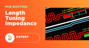
Length Tuning Impedance
Blog
What is the Impedance of Length-Tuning Structures?

Do length-tuning structures create an impedance discontinuity? The answer is an unequivocal “yes”, but it might not matter in your design depending on several factors. Applying a length-tuning structure is equivalent to changing the distance between the traces while meandering. Therefore, you will have a change in the odd-mode impedance of a single trace. The question then becomes: does this deviation in trace impedance in a length tuning structure matter?

Embedded thumbnail for Creating a Schematic Symbol - Placing Designators and Comments
How to create a Schematic Symbol
Creating a Schematic Symbol - Placing Designators and Comments

Placing your designator or comments can be done automatically, but that doesn’t mean they’re visible. We’ll walk you through how to make them visible and position them correctly no matter what orientation your symbol is with automatic positioning.

Embedded thumbnail for Creating a Schematic Symbol: Adding Additional Parts
How to create a Schematic Symbol
Creating a Schematic Symbol: Adding Additional Parts

Altium Designer makes it easy to add additional parts to your schematic library. We’ll show you how through copying and configuring your new components through the Pin Editor and the properties panel.

Tag
Schematic Compare
Blog
Schematic Compare

A design project doesn’t appear out of nowhere. The design process spreads over time, and project documents change. Schematic documents gradually become more complex, new functional blocks appear, and already finished parts can be modified and updated.

Embedded Capacitance Materials Overview
Blog
Embedded Capacitance Materials Overview

Capacitance is your friend whenever you need stable power integrity, which is why there is so much focus on decoupling capacitors. While these components are important and they can be used to provide targeted power integrity solutions to certain components, there is one specialty material used to supercharge capacitance in your PCB stackup or package substrate. 
How To Import Libraries and Manage Components With Altium 365
Blog
How To Import Libraries and Manage Components With Altium 365

The problems you can experience with components and libraries are endless. These problems are the most significant source of design issues and the biggest reason behind respins, costing companies untold amounts of lost profit annually.
If you want to have a better understanding of how to use Altium 365 to maintain a strong and centralized library that is free of problems and headaches, you may want to consider attending this lecture.

The High-Speed PCB Stackup Design Challenge
Blog
The High-Speed PCB Stackup Design Challenge

As much as we would like to build every high speed PCB perfectly, with ideal SI/PI/EMI characteristics, it isn’t always possible due to many practical constraints. Sometimes a stackup can be “good enough,” even for a high-speed PCB. This always comes from the need to balance engineering constraints, functional requirements, and the need to ensure signal and power integrity in a high-speed design, and finally to ensure compliance with EMC requirements.
How I Improved My Collaboration Efficiency with Altium 365
Blog
How I Improved My Collaboration Efficiency with Altium 365

Involving the whole team that will bring a product to completion early on in the development cycle is vital to efficient development. Design reviews with all the relevant parties are critical at each step of the design process, starting with high-level component selection, then through the schematic capture and PCB layout stages. 

Countersink and Counterbore
Blog
Countersink and Counterbore

Ergonomics and convenience are important issues when designing a printed circuit board and the device as a whole. A lot of Altium Designer tools are aimed at solving them. These include Countersink and Counterbore holes, which allow the use of various types of screws in the mounting holes of the board.

Migrating Data From Other Version Control Systems
Blog
Migrating Data From Other Version Control Systems

The development of electronic devices always involves the release of many different types of files. And these files are not static - they change as the project progresses. When filling a project with data, a user creates new files, modifies outdated files that have become irrelevant. Managing project data is a separate task, especially for large developments where several participants with different specializations are involved in the process.
Properties Panel Tuning
Blog
Properties Panel Tuning

High-speed PCBs often require tuning groups of tracks, both single and differential. Altium Designer includes powerful tools that allow you to solve such tasks quickly and with high quality. Study this document and achieve the desired result even faster.

Reflectionless Matching vs. Conjugate Matching: An Apparent Contradiction
Blog
Reflectionless Matching vs. Conjugate Matching: An Apparent Contradiction

There is one confusion related to impedance matching that comes up again and again, and it appears to be a fundamental confusion between reflection and power delivery. This leads to an apparent contradiction that arises when we try to generalize power delivery to wave reflection, despite the fact that the two were not meant to be related.

Properties Panel Routing
Blog
Properties Panel Routing

Routing is one of the most time-consuming stages of PCB design. Altium Designer has a large set of tools that allow you to do it as accurately and quickly as possible. This document will help you to learn how to manage your routing effectively and use it to its fullest extent.
Quarter-Wave Transformer Design For Real and Reactive Loads
Blog
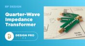
Quarter-Wave Transformer Design For Real and Reactive Loads

RF systems operate with specific impedance values across entire interconnects, including on PCBs. Not all RF components are packaged in integrated circuits with defined impedances, so impedance matching circuits and line sections are needed to ensure signal transmission between different sections of an interconnect. One of these impedance matching techniques is the quarter-wave impedance transformer, which can be implemented as a printed trace with specific impedance.
Schematic
Blog
Altium Designer 22.10 Update

We are happy to announce that the Altium Designer 22.10 update is now available. Altium Designer 22.10 continues to focus on improving the user experience, as well as performance and stability of the software, based on feedback from our users. Check out the key new features in the What's New section on the left side of this window!

Component Warpage Causes in a PCB
Blog
Component Warpage Causes in a PCB

A staff member at a PCB manufacturer once explained to me that they thought we were having an issue with a package warping. Unfortunately, component warping can occur both in a PCB and in components. In this article, we'll give an overview of warpage in a PCB, specifically in the circuit board and in the components.

Link Budget Calculator
Blog
RF Signal Chain and Link Budget Basics

If you're designing a wireless IoT device, and you know how to calculate the link budget, you can reasonably estimate whether your signal will reach its destination and be read by the receiver. To calculate the link budget, the designer needs to know something about all other sources of gain and loss in the system. Once link budget is determined, the designer can judge whether some modification is needed in their RF signal chain. 
How to Calculate SMD Pad Sizes?
Blog
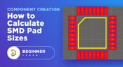
Best Methods for Calculating SMD Pad Size in PCB Design

SMD components require precisely sized pads for soldering during assembly. The designer is responsible for ensuring pad sizes are correct, either by calculating them and comparing with footprint data, looking through datasheets, or by memorizing SMD pad size standards. If you have a component and you don't have access to the footprint, and you decide to biuld the footprint yourself, what resources are available to ensure you have the correct pad size?

Can You Fix a Warped PCB?
Blog
Can You Fix a Warped PCB?

Before we get too deep into this article, I’ll give you the simple answer. You probably can’t fix warping in your PCB after it’s already been fabricated. You can prevent an unwarped board from becoming warped during assembly, but only as long as materials were selected properly and the board is put into reflow correctly. We’ll run over some of these points in this article, and I’ll examine some points that might help you recover a warped board.


Tag
NEW
Embedded thumbnail for Coming Soon: Advanced Via Fencing
New in Altium's Software
Coming Soon: Advanced Via Fencing

Coming soon to Altium software: Advanced Via Fencing gives you greater control over creating and managing shielding and stitching vias for RF and high-speed designs. Configure via fences directly from the Properties panel, follow traces or geometry edges, use stacked vias, define spacing and patterns, and preview the results before generating them.

NEW
Embedded thumbnail for 5 DC Power Integrity Myths That Ruin Your PCB Design
How-To's
5 DC Power Integrity Myths That Ruin Your PCB Design

DC power integrity plays a critical role in the reliability of nearly every power electronics board, yet common misconceptions can lead to costly design decisions. In this video, we break down five of the most common DC power integrity myths and explain what you really need to know for reliable power electronics design.

Embedded thumbnail for A fraction of a millimeter is the difference between a robot that fits and one that doesn't
Collaborative Engineering with Team Ribbot
A fraction of a millimeter is the difference between a robot that fits and one that doesn't

Check out the latest episode about Team Ribbot and see how they move design data between their electrical and mechanical tools without losing accuracy. Discover how Altium Designer and MCAD CoDesign help bring the boards, housings, and custom motors together right the first time with no surprises.

Embedded thumbnail for  HDI PCB Stackup Breakdown - Etching Weight Via Spacing, & More
How-To's
HDI PCB Stackup Breakdown - Etching Weight Via Spacing, & More

HDI PCB design depends on getting the stackup and manufacturing constraints right. In this deep dive, we examine a real HDI audio-interface board and explore common pitfalls, from how copper weight and etching affect minimum clearances to why solder mask slivers below 1 mil can cause manufacturing issues. You’ll also learn how proper board-edge clearance and copper pullback help protect SMD pads during routing.

Embedded thumbnail for  How do you review a robot design when your team is never in the same room?
Collaborative Engineering with Team Ribbot
How do you review a robot design when your team is never in the same room?

Team Ribbot’s engineers are spread across five states and juggle full-time jobs while building a 250-pound combat robot in their spare time. Discover how Altium Designer and Altium 365 keep the team connected, letting engineers open the live design from a laptop or phone, inspect the board in 3D, and leave comments directly on the design.

Embedded thumbnail for  Improve Visual Accuracy with True Arcs
New in Altium's Software
Improve Visual Accuracy with True Arcs

Discover how True Arc Rendering improves arc visualization in the PCB Editor and PCB Library Editor by displaying true arcs across 2D, 3D, and Board Planning modes. This provides a more accurate representation of board geometry and helps you work with curved features with greater precision throughout the design process.

Embedded thumbnail for Two engineers, one board, nobody's work gets wiped out
Collaborative Engineering with Team Ribbot
Two engineers, one board, nobody's work gets wiped out

When Team Ribbot’s electrical and mechanical engineers work on the same combat-robot design, unwanted changes can mean hours of lost work. See how Altium Designer and MCAD CoDesign let the team review and selectively accept changes, enabling seamless parallel collaboration across different locations and schedules.

Embedded thumbnail for Visualize and Refine Your Harness Designs
New in Altium's Software
Visualize and Refine Your Harness Designs

Create detailed views of bundle contents, control wire and cable paths, and rotate physical models to accurately represent the final harness assembly. These capabilities give you greater control over harness design and help ensure your digital model reflects the physical result.

Embedded thumbnail for Introducing Agentic Requirements Engineering
New in Altium's Software
Introducing Agentic Requirements Engineering

Discover a new way to work with Requirements Portal through Agentic Requirements Engineering. AI agents analyze your project data and surface proposals for your approval, reducing friction in requirements management and helping align your team's shared model with your design intent.

Embedded thumbnail for Simplify Rule Set Updates and Replacement
New in Altium's Software
Simplify Rule Set Updates and Replacement

Learn how to import rule sets with greater flexibility in Altium. When importing rules, you can add new rules to your existing set, replace only rules that match, or completely replace the current rule set giving you full control over how design rules are updated.

Embedded thumbnail for  How Team Ribbot fits 40 kW of power into a 250-pound combat robot
Collaborative Engineering with Team Ribbot
How Team Ribbot fits 40 kW of power into a 250-pound combat robot

What do you get when you pack the power of a small electric car into a combat robot with virtually no room to spare? In the first episode of our collaboration with Team Ribbot and Altium, explore how seamless ECAD-MCAD collaboration helps the team tackle complex design challenges, optimize high-performance designs, reduce errors, and bring products to life faster.

Embedded thumbnail for Just Released: Supplier Data Merging
New in Altium's Software
Just Released: Supplier Data Merging

Discover how the Supplier Data Merging feature brings together supplier information from your custom parts database and the Altium Parts Provider into a single, unified view. Access consolidated supplier data wherever supplier part numbers appear, including in ActiveBOM and during component selection.

Embedded thumbnail for How Altium’s Layer Stack Manager Actually Works
How-To's
How Altium’s Layer Stack Manager Actually Works

Take a look inside Altium's Layer Stack Manager and discover how its impedance calculator determines the ideal trace width for your target impedance. In this video, we break down the "black box" behind the calculation and show how the Simbeor-based field solver provides accurate results while eliminating the need for advanced field solver expertise.

Embedded thumbnail for Connect Requirements Directly to Your PCB Design
New in Altium's Software
Connect Requirements Directly to Your PCB Design

See how the Requirements Portal integration in Altium Designer simplifies requirements management by bringing system requirements directly into your PCB design workflow. Connect requirements to design documents, assign tasks, track verification in real time, and keep your entire team aligned with seamless synchronization in Altium 365.

Embedded thumbnail for SFP Connector Routing: High-Speed Differential Pair Design Tips
How-To's
SFP Connector Routing: High-Speed Differential Pair Design Tips

Discover practical SFP and SFP+ routing tips in our latest video, inspired by a real question from the Altium subreddit. We cover how aggressive serpentine length tuning can be, how to reduce impedance discontinuities in tight meanders, and how meandering influences mode conversion at 10G and higher data rates.

Embedded thumbnail for Handle High-Density PCB Layouts with Ease
New in Altium's Software
Handle High-Density PCB Layouts with Ease

Push the limits of PCB design with support for up to 128 signal layers, empowering the development of even the most complex, high-density boards.

Tag
Your search returns no results.