News & Updates


Blog
•
How to Get 3-port S-parameters From a 2-port VNA Measurement
S-parameters are fundamental quantities in signal integrity, and an ability to understand them from measurement or analysis is very important. If you have a 3-port network, like a power divider or circulator, it may appear that you must use a 3-port VNA to measure these S-parameters. It is always acceptable to measure between two ports, but you need to know what exactly it is you are measuring. In this article, we’ll look at the relationship between the true 3-port S-parameters with a 2-port measurement.


Blog
•
A Day in the Life of the PCB Manufacturing Process
Before implementing design for manufacturing, it is important to understand the underlying process behind producing a physical PCB. Regardless of the various technologies present in each facility, a large majority of industry-leading manufacturers follow a specific set of steps to turn your design from a drawing in a CAD application into a physical board. In this article, we'll cover the basics that designers need to know as part of our crash course series on PCB manufacturing.



Blog
•
Addressing Skew Sources in High Speed PCBs
If you compile a list of skew sources, you'll see that fiber weave-induced skew is only one entry on a long list of skew sources. We'll look at this list of possible skew sources below, and we'll see how they affect the operation of your PCB. From the list below, we'll see that some of these issues with skew are not simply solved by paying attention to the fiber weave construction in a PCB substrate.
Blog
•
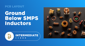
Should Ground Be Placed Below Inductors in Switching Regulators?
We love answering questions from our readers and YouTube viewers, and one of the recent questions we received relates to EMI from switching elements in a switching regulator is "Should a cutout be placed below the inductor in a switching regulator circuit?". Despite the variations in inductors and their magnetic behavior, there are some general principles that can be used to judge the effects of placing ground near inductors in switching regulator circuits. We’ll look at some of these principles in this article

Blog
•
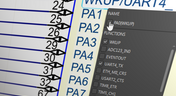
Altium Designer 22.6 Update
We are happy to announce that the Altium Designer 22.6 update is now available. Altium Designer 22.6 continues to focus on improving the user experience, as well as performance and stability of the software, based on feedback from our users. Check out the key new features in the What's New section on the left side of this window!

Blog
•
Join PCB Design Review Competition from Altium
Find 9 mistakes in a PCB design and get added into the lucky draw to win a prize from Altium!

Blog
•
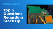
SAP (Semi-Additive PCB Process) – Top 5 Questions Regarding Stack Up
This Semi-Additive Process is an additional tool in the PCB fabricators' toolbox that enables them to provide feature sizes for trace width and spacing that are 25 microns, (1 mil) and below depending on the fabricators' imaging equipment. This provides much more flexibility to breakout out tight BGA areas and the ability to shrink overall circuit size and/ or reduce the number of circuit layers in the design. As the PCB design community embraces the benefits of this new printed circuit board fabrication technique, there are of course many questions to be answered.



Blog
•
Improving Supply Chain Success with BOM Management
It’s no secret that component shortages have become more frequent this year. In fact, countries around the world are losing billions in revenue due to supply issues. Having the right components on hand is more crucial than ever as availability, obsolescence, counterfeit products and environmental non-compliance risks continue to grow. Fortunately, many shortages can be avoided by introducing proactive supply chain practices.
Blog
•
What is the Impedance of Length-Tuning Structures?
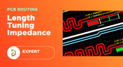
Do length-tuning structures create an impedance discontinuity? The answer is an unequivocal “yes”, but it might not matter in your design depending on several factors. Applying a length-tuning structure is equivalent to changing the distance between the traces while meandering. Therefore, you will have a change in the odd-mode impedance of a single trace. The question then becomes: does this deviation in trace impedance in a length tuning structure matter?



Blog
•
The Role of Automation & Robotics in Wire Harness Assembly
Our new article highlights how automation and robotics are transforming wire harness assembly, improving efficiency, precision, and cost-effectiveness. Technologies like robotic wire handling and AI-driven testing are paving the way for smarter production. However, challenges like custom designs and high costs still persist.

Blog
•
Best Practices for Electronics Project Management - Part 1
Check out the first part of "Best Practices for Electronics Project Management" by Rafał Stępień. It offers valuable advice on enhancing team communication and documentation in hardware design projects.

Blog
•
Wiring for the Final Frontier: A Guide to Space-Grade Harness Design
Wiring harnesses are mission-critical in space systems, requiring strict adherence to ECSS-Q-ST-70-61C and NASA-STD-8739.4A. In "Wiring for the Final Frontier: A Guide to Space-Grade Harness Design", Kamil Jasiński explores key design principles, material selection, and testing to ensure reliability in extreme environments.

Blog
•
The Future of Wire Harnesses in the Electric Vehicle and Electronics Era
Discover how wire harnesses are evolving to meet the demands of electric vehicles and modern electronics. Our latest article explores key trends like higher voltages, lightweight designs, and smart harnesses, along with challenges such as cost and supply chain issues.
Blog
•
Mastering EMI Control in PCB Design: Decoupling Strategies for PDN
Dario Fresu explores effective decoupling strategies for power distribution networks (PDNs) to minimize EMI in PCB designs. The article covers techniques like decoupling capacitors and power planes to ensure stable power delivery for integrated circuits.

Blog
•
Building Your Own Android Device with a Raspberry Pi
Learn how to turn a Raspberry Pi into a custom Android device. This guide covers hardware selection, software setup, and troubleshooting common issues.

Blog
•
How PCB Design Engineers Can Securely Share Design Files with External Teams
Learn how PCB design engineers can securely share design files with team members, clients, and manufacturers. Marek Orzeł explores best practices and tools to protect your intellectual property while ensuring efficient collaboration.

Blog
•
OEMs and Harness Manufacturers: Building Strong Collaboration for Success
Strong partnerships between OEMs and harness manufacturers are key to efficient, high-quality product development. In this article, Krishna Sundaram shows how collaboration, clear communication, and the right design tools can streamline the harness manufacturing process and drive success.
Blog
•
Ideal Rectifier Bridge
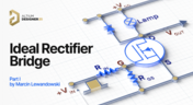
Read Marcin Lewandowski's article explaining how MOSFETs are replacing traditional diodes for reverse polarity protection. Step into the future of energy-efficient electronics!
Blog
•
Master Your Circuit Design: Dive into Worst Case Analysis
Dive into Worst Case Analysis techniques with Kamil Jasiński and ensure the reliability of your circuits. Master sensitivity analysis, Monte Carlo simulations, and more to confidently address real-world challenges.
Blog
•
Overview of the Gerber X3 File Format
Want to learn how the Gerber X3 file format simplifies data exchange by unifying assembly and fabrication details in a single file? This article explores the format and its role in streamlining PCB manufacturing.

Blog
•
Save Time and Prevent Errors in Cable Harness Design Today
Our new article explores best practices and tools for streamlining cable harness design workflows. Learn how to minimize errors, save time, and enhance collaboration by leveraging advanced features in Altium Designer.
Blog
•
Mastering EMI Control in PCB Design: How to Design PCBs for Low EMI
This article by Dario Fresu delves into effective techniques for designing PCBs to reduce electromagnetic interference (EMI). It covers key topics such as stackup selection, routing strategies, and grounding best practices, offering actionable insights for improved performance.

Blog
•
Altium and Renesas’ Role in Enabling Economy 4.0 is the Subject of New Documentary
Altium and Renesas are featured in a new CBS-produced documentary exploring how digitalization and cloud platforms are revolutionizing electronics production for Economy 4.0, driving efficiency and accelerating innovation.

Blog
•
Avoid Wiring Errors with Tools Tailored for Harness-to-PCB Integration
Discover how to streamline your wiring projects with advanced harness and PCB integration tools in Altium Designer. This article explores techniques to prevent wiring errors, enhance collaboration, and ensure accurate design documentation for complex projects.

Blog
•
Happy Holidays!!!
Altium wishes you all the best this holiday season! May this time be filled with joy, laughter, and cherished moments with your family and friends. We also extend our warmest wishes for a Happy New Year 2025!
















Your search returns no results.


