News & Updates


Blog
•
DFM in PCB Material Selection
Every design should begin with selecting the materials that will appear in the PCB stackup, as well as arranging layers in the stackup to support layout and routing. This section of our PCB manufacturing andc DFM crash course focuses on selecting the right materials for your PCB design. Materials should be selected given the particular design requirements outlined in your specifications.

Blog
•
How to Start an FPGA PCB Layout For Your Embedded System
FPGAs come in quad or BGA packages that can be difficult to floorplan, especially with the high number of I/Os often implemented in these components. FPGAs offer a lot of advantages in terms of their reconfigurability, but they can require a lot of effort to layout and route without headaches. If you’ve never worked with an FPGA in your PCB layout, we have some guidelines that can help you get started.


Blog
•
How to Get 3-port S-parameters From a 2-port VNA Measurement
S-parameters are fundamental quantities in signal integrity, and an ability to understand them from measurement or analysis is very important. If you have a 3-port network, like a power divider or circulator, it may appear that you must use a 3-port VNA to measure these S-parameters. It is always acceptable to measure between two ports, but you need to know what exactly it is you are measuring. In this article, we’ll look at the relationship between the true 3-port S-parameters with a 2-port measurement.


Blog
•
A Day in the Life of the PCB Manufacturing Process
Before implementing design for manufacturing, it is important to understand the underlying process behind producing a physical PCB. Regardless of the various technologies present in each facility, a large majority of industry-leading manufacturers follow a specific set of steps to turn your design from a drawing in a CAD application into a physical board. In this article, we'll cover the basics that designers need to know as part of our crash course series on PCB manufacturing.


Blog
•
Addressing Skew Sources in High Speed PCBs
If you compile a list of skew sources, you'll see that fiber weave-induced skew is only one entry on a long list of skew sources. We'll look at this list of possible skew sources below, and we'll see how they affect the operation of your PCB. From the list below, we'll see that some of these issues with skew are not simply solved by paying attention to the fiber weave construction in a PCB substrate.

Blog
•
Should Ground Be Placed Below Inductors in Switching Regulators?
We love answering questions from our readers and YouTube viewers, and one of the recent questions we received relates to EMI from switching elements in a switching regulator is "Should a cutout be placed below the inductor in a switching regulator circuit?". Despite the variations in inductors and their magnetic behavior, there are some general principles that can be used to judge the effects of placing ground near inductors in switching regulator circuits. We’ll look at some of these principles in this article


Blog
•
Altium Designer 22.6 Update
We are happy to announce that the Altium Designer 22.6 update is now available. Altium Designer 22.6 continues to focus on improving the user experience, as well as performance and stability of the software, based on feedback from our users. Check out the key new features in the What's New section on the left side of this window!


Blog
•
Join PCB Design Review Competition from Altium
Find 9 mistakes in a PCB design and get added into the lucky draw to win a prize from Altium!


Blog
•
SAP (Semi-Additive PCB Process) – Top 5 Questions Regarding Stack Up
This Semi-Additive Process is an additional tool in the PCB fabricators' toolbox that enables them to provide feature sizes for trace width and spacing that are 25 microns, (1 mil) and below depending on the fabricators' imaging equipment. This provides much more flexibility to breakout out tight BGA areas and the ability to shrink overall circuit size and/ or reduce the number of circuit layers in the design. As the PCB design community embraces the benefits of this new printed circuit board fabrication technique, there are of course many questions to be answered.


Blog
•
Altium Designer 20 Changed My Layout Design Routines
I just finalized my first PCB design using Altium Designer 20. At the same time, I tested some new AD20 features, and in this article, I’ll share my thoughts about new layout design features which made the biggest impression for me: sliding, and any-angle routing.
Blog
•
Designing for Antenna Isolation in Your Wireless System
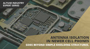
Anyone who has taken apart an old cell phone or designs IoT devices knows multiple communication capabilities are present in these designs, each requiring different antennas. The RF designer should already take precautions for interconnect isolation, but antenna isolation is just as important when modeling and designing wireless systems.

Blog
•
PCB Trace and Pad Clearance: Low vs. High Voltage
High voltage/high current designs carry safety requirements which need to be met by designers. Similarly, high speed designs need to have suppressed crosstalk in order to ensure signal integrity. The key design aspects that relate to both areas are your PCB trace clearance and pad clearance values. These design choices are critical for balancing safety, noise suppression, and manufacturability.
Blog
•
Getting Through PCB DFM
In this article, we’ll discuss the key design features to implement, and steps to take prior to fabrication that will help prevent some DFM process pain.
Blog
•
Level Up Your Design Skills - Altium Designer Getting Started User Guide Update
We are happy to announce the new update of our Altium Designer Getting Started User Guide. Whether you are new to Altium Designer or you want to brush up on some topics, the Altium Designer Getting Started User Guide will take you from a beginner to a master in PCB design.
This is only the beginning! This guide will be updated with new information based on user feedback. Let’s first go over the contents of the guide.

Blog
•
Modeling Copper Foil Roughness in Altium Designer's Impedance Profiler
With the new layer stack manager in Altium Designer®, you can now include copper foil roughness factors directly in your impedance calculator. This is quite easy to do in the layer stack manager, but it begs the question: what exactly is the copper roughness factor? Which value should be used for your interconnects?

Blog
•
High-Speed Signal Routing: The 5 Important Constraints
After you capture your schematic as an initial layout and create an initial component arrangement, it’s time to define your routing constraints. Doing this early will allow your DRC engine to spot rules violations before you finish your layout. Likewise, you’ll be able to modify the default rule set to meet your layout requirements. Here are the important routing constraints you’ll need to check before you start routing your board.
Blog
•
CoDesigner and MCAD Component Placement On-Demand Webinar
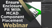
Learn how to place components from the MCAD side and synchronize them with Altium Designer ECAD models, designators, and sourcing data to simplify your design process.
Blog
•
How to Create a PCB Manufacturing Cost Estimation
Some manufacturers have very convenient PCB manufacturing cost estimation calculators you can use, but the real costs depend on a number of factors. If you’re an entrepreneur and you’re producing your own boards, or you are managing manufacturing, testing, and delivery for a new project, it’s your job to help clients understand the primary cost drivers for new boards. Here’s how you can get an estimate of your fabrication costs, both for local and overseas manufacturers.
Blog
•
PCB Mountable Connectors: SMD vs. Through-hole
Selecting a connector is as much an art as it is a science. The artistic side is all about aesthetics and satisfying clearances, while the scientific side is all about signal integrity. For PCB mountable connectors, you’ll need to choose between surface-mounted or through-hole connectors, and you’ll need to consider how each type affects signal integrity in your application. Here’s what you need to think about beyond the standard connector specifications.

Blog
•
PCB Via Current-Carrying Capacity: How Hot is Too Hot?
Trace and via current-carrying capacity are legitimate design points to focus on when designing a new board that will carry high current. The goal is to keep conductor temperatures below some appropriate limit, which then helps keep components on the board cool.
Blog
•
How to Maximize Copper in Your PCB Design: The Pros and Cons of Copper Pouring Versus Placing
There is a saying in copper pour PCB design, “Copper is free.” It means a PCB editor designer must think in reverse. A board starts off as solid copper, and the copper you don’t want is removed. It is faster to build, less consumptive, and less expensive to make a board that is mostly copper as compared to the same size board that is mostly bare. Picking the correct technique will make the difference between an effortless or frustrating experience.

Blog
•
Top 5 PCB Design Guidelines Every PCB Designer Needs to Know
What’s the key to designing a board that’s realistic on paper and in physical form? Let’s explore the top 5 design guidelines that you need to know to design your next manufacturable, functional and reliable PCB.
Blog
•
May 14, 2020
How to Highlight Nets in Altium Designer to Simplify Schematic and PCB Designs
Highlighting nets will help you simplify your schematic and PCB design. In Altium , there are multiple options that enable you to leverage this capability to simplify the verification of connections and circuit paths and make sure that the design you send to your manufacturer accurately reflects the printed circuit board you need built.

Blog
•
May 12, 2020
Keep Your Altium Designer PCB Layout in Line with Grids and Grid-Selection Shortcuts
The grid system in a printed circuit board design CAD system really is your friend, and if you haven’t taken the time to get properly introduced yet let me help you with that.

Blog
•
May 7, 2020
How to Panelize Your PCBs Before Lunch with Altium Designer
Whether you have a slew of PCBs to mass produce for your customers or a handful of project boards you wish to prototype all in one simple swoop, panelization is an effective way to bring high amounts of efficiency to your production.




Your search returns no results.


