News & Updates
Blog
•
Altium Designer 22.8 Update
We are happy to announce that the Altium Designer 22.8 update is now available. Altium Designer 22.8 continues to focus on improving the user experience, as well as performance and stability of the software, based on feedback from our users. Check out the key new features in the What's New section on the left side of this window!

Blog
•
What is Hybrid Beamforming?
In this article, we’ll look at beamforming implementation in an advanced method combining analog and digital techniques, known as hybrid beamforming. This method blends both digital and analog techniques to create multiple beams and thus reach multiple users with varying intensities. In the case of an RF imaging system or a radar system, hybrid beamforming in a MIMO technique also allows tracking of multiple targets with adjustable resolution.

Blog
•
Why Most Via Impedance Calculators Are Inaccurate
The problem with every via impedance calculator that I have seen is simple: they are incomplete or totally wrong. The “incomplete” part refers to a lack of context; these calculators can roughly reproduce a well-known estimate from a legend like Howard Johnson in his Digital Design textbooks. However, these calculators never provide insight into what they are actually calculating, or where the calculated via impedance is accurate. Keep reading to see why these calculators get it so wrong, as well as the context surrounding via impedance.



Blog
•
Buck Converter Simulation in Altium Designer
When designing high power circuits (usually very high voltage and/or current), you’ll need to create a regulator from scratch and place it in your PCB layout. It's also the case that you may want to model a real component using discretes in a simulation in order to qualify the system's expected operating regime. As part of buck converter design, you can easily run a buck converter simulation directly in Altium Designer’s schematic editor. Here’s how you can access these features in the newest version of Altium Designer.

Blog
•
Overview of the PCIe 6.0 Standard
Just as you get used to PCIe 5.0, they decide to release another standard! The newest iteration of PCIe is Gen6, or PCIe 6.0. PCIe 6.0 brings a doubling of channel bandwidth through introduction of PAM-4 as the signaling method in high-speed differential channels. This signaling method is a first for PCIe, and it’s an important enabler of the doubled data rate we see in the current standard. In this article, I’ll run over the important points in the standard and what PCB designers can expect when designing these channels.


Blog
•
SPI vs. I2C: How to Choose the Best Protocol for Your Memory Chips
One of the common implementations of SPI and I2C in a PCB layout is as a protocol for reading and writing to an external Flash memory. Flash chips are a very common component in embedded systems and can offer high capacities of non-volatile memory up to Gb values. When choosing a memory chip, you'll want to match the application requirements and functionality with the bus speed you need for read and write operations in your memory chip. There is also the matter of the type of Flash memory you'll need to access (NOR vs. NAND).
Blog
•
Is There an SPI Trace Impedance Requirement?
There is no SPI trace impedance requirement? The reality is that SPI lines only start to need impedance control when the length of the interconnect becomes very long. And because there is no specific impedance requirement in the bus, you have some freedom in channel design and termination. So what exactly qualifies as “very long” and when is some termination method needed? We’ll break it down in this article.



Blog
•
The Skin Effect, Current Density, and the Electromagnetic Field
During this year's AltiumLive CONNECT event, I recall receiving an interesting question about the skin effect and the distribution of current due to the presence of ground in coplanar transmission lines. In this article, we'll look at the electric field around a transmission line carrying a signal, and how this might be impacted by the skin effect.

Blog
•
What You Need for PCB Packaging and Shipping
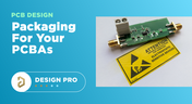
When you get your PCBA back from an assembler, you’ll notice the packaging materials used to pack and ship the PCBA. Those materials are specific to electronics, and if you build products on behalf of clients, it’s important to know the packaging materials used for packing and shipping electronics. In this article I’ll show the main set of materials and equipment used to package electronics assemblies.



Blog
•
How to Make PCB Gerber Files in Altium Designer Step-by-Step
Once you've got your PCB layout finished and you're ready to start preparing for manufacturing, one of the critical steps is to create PCB Gerber files. When you're ready to create your Gerber files, you need the right set of CAM processor tools that can take data from your PCB layout. In this article, we'll guide you through this process of how to make PCB Gerber files and show some example tasks you might need to perform to generate them.
NEW
Blog
•
Breaking the Multiboard Bottleneck: How Unified Design Solves ECAD–MCAD Disconnects
This article examines how fragmented ECAD-MCAD workflows create costly misalignments, late-stage conflicts, and inefficiencies in multiboard system design. It shows how unified, collaborative platforms enable real-time synchronization, digital twins, and cross-domain visibility to eliminate rework and streamline development.

Blog
•
Altium Designer vs. Flux For Professional PCB Projects
Choosing the right PCB tool can define your entire design workflow. Discover how Altium Designer empowers professional product development, while Flux.ai keeps things simple for fast experimentation.
Blog
•
Rigid-Flex Stackups: Where Good Designs Go Wrong Before Layout Even Starts
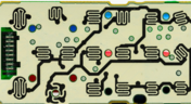
Rigid-flex stackups are more complex than they seem and getting them wrong early can lead to costly failures later. This article shows how smart decisions around materials, transitions, and layer structure help ensure a reliable design.

Blog
•
From Complexity to Clarity: Smart Design Reviews for Agile Engineering Teams
Understand how structured design reviews within Altium Agile Teams enhance visibility, traceability, and cross-team collaboration. This webinar highlights methods to detect issues early and optimize your development workflow.

Blog
•
Building a Local-LLM Datasheet Extractor for IC Driver Development
Parsing long datasheets manually slows down embedded development and introduces errors. This article shows how to use a local LLM pipeline to convert datasheets into structured data that speeds up driver creation.

Blog
•
Types of Simulation Tools For PCBs
PCB simulation isn’t one-size-fits-all and that’s where it gets interesting! Discover the wide range of tools available, from quick circuit checks to advanced multiphysics simulations, and how they help you design with confidence.

Blog
•
Wiring the Future: The Shift to Unified Electromechanical Design
This article explores the shift from PCB-centric design to complex, system-level development where wiring and harnesses play a critical role in product performance. It highlights how unified electromechanical workflows and bi-directional ECAD–MCAD integration improve accuracy, reduce delays, and ensure reliable, production-ready designs.
Blog
•
Best Tools For PCB DFM Checks
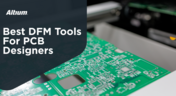
Want to catch manufacturability issues before they turn into expensive delays? Discover the essential DFM tools from real-time checks to post-layout analysis that help you get your PCB right the first time.

Blog
•
Eliminate Your Design Friction with Agile Teams
Design friction from scattered data and disconnected tools slows down PCB development and leads to rework. This webinar shows how Agile Teams streamlines collaboration, aligns domains, and helps teams deliver faster with fewer errors.

Blog
•
What Is an Integrated Design Environment for Electronics?
Using multiple disconnected tools slows down PCB development and increases the risk of errors. This article shows how an integrated environment keeps all design data connected, enabling faster workflows and fewer late-stage issues.

Blog
•
What is the Best Cloud PCB Design Software?
Not all cloud PCB tools are created equal, especially when design complexity increases. This article breaks down key differences between cloud-native and hybrid solutions, helping engineers choose the right approach for performance and scalability.

Blog
•
From Rework to Revenue: Digital PCB DFMA
This article explores how traditional, manual DFMA workflows lead to costly rework, delays, and poor collaboration across engineering teams. It shows how a connected, digital approach enables better data integrity, faster design cycles, and improved manufacturing outcomes.

Blog
•
Introducing Octopart Discover: From Part Search to Solutions Discovery
Octopart has announced Octopart Discover, a new platform that shifts electronic component search toward system-level solution discovery. The tool connects design intent with relevant options, enabling engineers to evaluate tradeoffs and identify the best-fit solutions more efficiently.

Blog
•
How to Choose the Right Components for Your BOM
A strong BOM can make the difference between smooth production and costly delays. Discover a practical approach to choosing components that stay available, meet compliance requirements, and keep your project on schedule.
Blog
•
From Scattered Requirements to Confident Product Development
See how the Requirements Portal transforms disconnected requirements into a single, live source of truth that engineers can trust at every stage of a project! Real customer stories in the article prove it’s already helping teams cut down on rework and bring products to market faster.

Blog
•
What is the Best PCB Design Tool For Students?
Students need PCB software that’s intuitive, affordable, and useful for building real skills. This article compares the strengths and weaknesses of leading design tools, from hobbyist platforms to industry-standard software.


Your search returns no results.


