News & Updates
Blog
•
How I Improved My Collaboration Efficiency with Altium 365
Involving the whole team that will bring a product to completion early on in the development cycle is vital to efficient development. Design reviews with all the relevant parties are critical at each step of the design process, starting with high-level component selection, then through the schematic capture and PCB layout stages.



Blog
•
Countersink and Counterbore
Ergonomics and convenience are important issues when designing a printed circuit board and the device as a whole. A lot of Altium Designer tools are aimed at solving them. These include Countersink and Counterbore holes, which allow the use of various types of screws in the mounting holes of the board.


Blog
•
Migrating Data From Other Version Control Systems
The development of electronic devices always involves the release of many different types of files. And these files are not static - they change as the project progresses. When filling a project with data, a user creates new files, modifies outdated files that have become irrelevant. Managing project data is a separate task, especially for large developments where several participants with different specializations are involved in the process.


Blog
•
Properties Panel Tuning
High-speed PCBs often require tuning groups of tracks, both single and differential. Altium Designer includes powerful tools that allow you to solve such tasks quickly and with high quality. Study this document and achieve the desired result even faster.

Blog
•
Reflectionless Matching vs. Conjugate Matching: An Apparent Contradiction
There is one confusion related to impedance matching that comes up again and again, and it appears to be a fundamental confusion between reflection and power delivery. This leads to an apparent contradiction that arises when we try to generalize power delivery to wave reflection, despite the fact that the two were not meant to be related.

Blog
•
Properties Panel Routing
Routing is one of the most time-consuming stages of PCB design. Altium Designer has a large set of tools that allow you to do it as accurately and quickly as possible. This document will help you to learn how to manage your routing effectively and use it to its fullest extent.

Blog
•
Quarter-Wave Transformer Design For Real and Reactive Loads
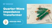
RF systems operate with specific impedance values across entire interconnects, including on PCBs. Not all RF components are packaged in integrated circuits with defined impedances, so impedance matching circuits and line sections are needed to ensure signal transmission between different sections of an interconnect. One of these impedance matching techniques is the quarter-wave impedance transformer, which can be implemented as a printed trace with specific impedance.


Blog
•
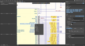
Altium Designer 22.10 Update
We are happy to announce that the Altium Designer 22.10 update is now available. Altium Designer 22.10 continues to focus on improving the user experience, as well as performance and stability of the software, based on feedback from our users. Check out the key new features in the What's New section on the left side of this window!
Blog
•
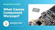
Component Warpage Causes in a PCB
A staff member at a PCB manufacturer once explained to me that they thought we were having an issue with a package warping. Unfortunately, component warping can occur both in a PCB and in components. In this article, we'll give an overview of warpage in a PCB, specifically in the circuit board and in the components.
Blog
•
RF Signal Chain and Link Budget Basics
If you're designing a wireless IoT device, and you know how to calculate the link budget, you can reasonably estimate whether your signal will reach its destination and be read by the receiver. To calculate the link budget, the designer needs to know something about all other sources of gain and loss in the system. Once link budget is determined, the designer can judge whether some modification is needed in their RF signal chain.
Blog
•
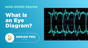
What is an Eye Diagram?
The eye diagram is a useful measurement or simulation as part of channel compliance. The measurement shows many different factors that can affect signal behavior simultaneously, ultimately allowing for qualification of errors and losses in a channel. In this article, I’ll run over some of the fundamental measurements that you could manually extract from an eye diagram and how they reveal some strategies for improving channel designs.

Blog
•
What Skills Are Needed to be a PCB Layout Designer?
To readers who have been working in the PCB industry for most of your career, you have probably seen a very diverse group of professionals with varied skill sets and backgrounds. Designers might get started as engineers or as technicians, and some designers learn how to create beautiful PCB layouts in university. No matter how you got into PCB design, there are some important skills to know that will take you a long way towards advancing your career.
Blog
•
Beginner PCB Design Mistakes and How To Avoid Them
When starting out with PCB design, it’s common to treat the process as simply ‘connecting the dots’: as long as connections are made, it’s not particularly important how these connections are made. Having reviewed quite a number of PCBs of other PCB design engineers over the last few years, there are common, unfortunately erroneous, occurrences between a lot of them. This article aims to illustrate the top five beginner PCB design mistakes and what we can do to avoid making them. Let’s get started!
Blog
•
SAP (Semi-Additive PCB Process) – Top 5 Questions Regarding Stack Up
As the PCB design community embraces the benefits of this new printed circuit board fabrication technique, there are of course many questions to be answered. Today’s blog will address some of the most commonly asked questions related to circuit layer stack up as people are introduced to this new technology.
Blog
•
Altium Designer 22.9 Update
We are happy to announce that the Altium Designer 22.9 update is now available. Altium Designer 22.9 continues to focus on improving the user experience, as well as performance and stability of the software, based on feedback from our users. Check out the key new features in the What's New section on the left side of this window!
Blog
•
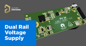
Dual Rail Voltage Supply
The highest performing operational amplifiers often need a split supply with positive and negative voltages connected to the op amps supply rails. In this project, we’re going to be building a positive/negative dual rail power supply for a differential oscilloscope probe I’m designing. I’m making the power supply a separate project, as a dual rail supply is quite useful to have, and I’m sure I’ll find multiple uses for it in the future.
Blog
•
Library Importer Improvements (former Library Migrator)
Importing file-based libraries from your local computer or network drive to your Altium 365 workspace can be done using the Library Importer. Altium’s Library Migrator was renamed Library Importer—the feature’s name was changed to conform more closely to the tool’s purpose. Not only is its name new, but our team has also made several user experience improvements. We have updated the documentation to reflect this change.

Blog
•
How to Select Copper Foil for High-Frequency PCB Design
The PCB materials industry has spent significant amounts of time developing materials that provide lowest possible signal loss for products with RF applications. For high speed and high frequency designs, losses will limit signal propagation distance and distort signals, and it will create an impedance deviation that can be seen in TDR measurements. In this article, we'll look at the balance between copper foil losses and other types of losses in a PCB, as well as some strategies that are commonly used to overcome roughness.
Blog
•
Altium Designer 22.8 Update
We are happy to announce that the Altium Designer 22.8 update is now available. Altium Designer 22.8 continues to focus on improving the user experience, as well as performance and stability of the software, based on feedback from our users. Check out the key new features in the What's New section on the left side of this window!
Blog
•
What is Hybrid Beamforming?
In this article, we’ll look at beamforming implementation in an advanced method combining analog and digital techniques, known as hybrid beamforming. This method blends both digital and analog techniques to create multiple beams and thus reach multiple users with varying intensities. In the case of an RF imaging system or a radar system, hybrid beamforming in a MIMO technique also allows tracking of multiple targets with adjustable resolution.

Blog
•
Why Most Via Impedance Calculators Are Inaccurate
The problem with every via impedance calculator that I have seen is simple: they are incomplete or totally wrong. The “incomplete” part refers to a lack of context; these calculators can roughly reproduce a well-known estimate from a legend like Howard Johnson in his Digital Design textbooks. However, these calculators never provide insight into what they are actually calculating, or where the calculated via impedance is accurate. Keep reading to see why these calculators get it so wrong, as well as the context surrounding via impedance.
Blog
•
Buck Converter Simulation in Altium Designer
When designing high power circuits (usually very high voltage and/or current), you’ll need to create a regulator from scratch and place it in your PCB layout. It's also the case that you may want to model a real component using discretes in a simulation in order to qualify the system's expected operating regime. As part of buck converter design, you can easily run a buck converter simulation directly in Altium Designer’s schematic editor. Here’s how you can access these features in the newest version of Altium Designer.
Blog
•
Overview of the PCIe 6.0 Standard
Just as you get used to PCIe 5.0, they decide to release another standard! The newest iteration of PCIe is Gen6, or PCIe 6.0. PCIe 6.0 brings a doubling of channel bandwidth through introduction of PAM-4 as the signaling method in high-speed differential channels. This signaling method is a first for PCIe, and it’s an important enabler of the doubled data rate we see in the current standard. In this article, I’ll run over the important points in the standard and what PCB designers can expect when designing these channels.
Blog
•
SPI vs. I2C: How to Choose the Best Protocol for Your Memory Chips
One of the common implementations of SPI and I2C in a PCB layout is as a protocol for reading and writing to an external Flash memory. Flash chips are a very common component in embedded systems and can offer high capacities of non-volatile memory up to Gb values. When choosing a memory chip, you'll want to match the application requirements and functionality with the bus speed you need for read and write operations in your memory chip. There is also the matter of the type of Flash memory you'll need to access (NOR vs. NAND).
Blog
•
Is There an SPI Trace Impedance Requirement?
There is no SPI trace impedance requirement? The reality is that SPI lines only start to need impedance control when the length of the interconnect becomes very long. And because there is no specific impedance requirement in the bus, you have some freedom in channel design and termination. So what exactly qualifies as “very long” and when is some termination method needed? We’ll break it down in this article.

Blog
•
The Skin Effect, Current Density, and the Electromagnetic Field
During this year's AltiumLive CONNECT event, I recall receiving an interesting question about the skin effect and the distribution of current due to the presence of ground in coplanar transmission lines. In this article, we'll look at the electric field around a transmission line carrying a signal, and how this might be impacted by the skin effect.







Your search returns no results.


