News & Updates



Blog
•
Schematic Compare
A design project doesn’t appear out of nowhere. The design process spreads over time, and project documents change. Schematic documents gradually become more complex, new functional blocks appear, and already finished parts can be modified and updated.

Blog
•
Embedded Capacitance Materials Overview
Capacitance is your friend whenever you need stable power integrity, which is why there is so much focus on decoupling capacitors. While these components are important and they can be used to provide targeted power integrity solutions to certain components, there is one specialty material used to supercharge capacitance in your PCB stackup or package substrate.
Blog
•
How To Import Libraries and Manage Components With Altium 365
The problems you can experience with components and libraries are endless. These problems are the most significant source of design issues and the biggest reason behind respins, costing companies untold amounts of lost profit annually.
If you want to have a better understanding of how to use Altium 365 to maintain a strong and centralized library that is free of problems and headaches, you may want to consider attending this lecture.


Blog
•
The High-Speed PCB Stackup Design Challenge
As much as we would like to build every high speed PCB perfectly, with ideal SI/PI/EMI characteristics, it isn’t always possible due to many practical constraints. Sometimes a stackup can be “good enough,” even for a high-speed PCB. This always comes from the need to balance engineering constraints, functional requirements, and the need to ensure signal and power integrity in a high-speed design, and finally to ensure compliance with EMC requirements.
Blog
•
How I Improved My Collaboration Efficiency with Altium 365
Involving the whole team that will bring a product to completion early on in the development cycle is vital to efficient development. Design reviews with all the relevant parties are critical at each step of the design process, starting with high-level component selection, then through the schematic capture and PCB layout stages.



Blog
•
Countersink and Counterbore
Ergonomics and convenience are important issues when designing a printed circuit board and the device as a whole. A lot of Altium Designer tools are aimed at solving them. These include Countersink and Counterbore holes, which allow the use of various types of screws in the mounting holes of the board.


Blog
•
Migrating Data From Other Version Control Systems
The development of electronic devices always involves the release of many different types of files. And these files are not static - they change as the project progresses. When filling a project with data, a user creates new files, modifies outdated files that have become irrelevant. Managing project data is a separate task, especially for large developments where several participants with different specializations are involved in the process.


Blog
•
Properties Panel Tuning
High-speed PCBs often require tuning groups of tracks, both single and differential. Altium Designer includes powerful tools that allow you to solve such tasks quickly and with high quality. Study this document and achieve the desired result even faster.
Blog
•
Reflectionless Matching vs. Conjugate Matching: An Apparent Contradiction
There is one confusion related to impedance matching that comes up again and again, and it appears to be a fundamental confusion between reflection and power delivery. This leads to an apparent contradiction that arises when we try to generalize power delivery to wave reflection, despite the fact that the two were not meant to be related.
Blog
•
How to Design Your PCB Test Coupon and What You Can Test
As the operating speed of components has increased, controlled impedance is becoming more common in digital, analog, and mixed-signal systems. If the controlled impedance value for an interconnect is incorrect, it can be very difficult to identify this problem during an in-circuit test. However, testing is normally performed on a PCB test coupon, which is manufactured on the same panel as the PCB. If you want to get through board spins quickly and aid future designs, you might consider designing a test coupon and keeping it handy for future designs.

Blog
•
Altium DbLibs and Electronic Components in the Cloud with Altium Designer 20.1
Altium’s DbLib support is one of the oldest and most loved features of Altium Designer for managing electronic components and their data. They’ve been present in the software world since before I could fathom the existence of Ohm’s law. Altium 20.1’s new Component Sync feature allows you to synchronize virtually any database or database Library with Altium 365, taking advantage of both approaches strengths.
Blog
•
What is a Schematic Netlist for Your PCB?
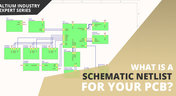
If you’ve created your next great schematic, there is a lot going on behind the scenes in your design software. A schematic netlist is one of the central pieces of information that will be used in multiple features in your design software to create a real PCB. Your schematic netlist provides both electrical connectivity information, and reflects the functional structure of your design data in a single set of data.
Blog
•
How to Select an Inductor for a Buck Converter
An SMPS is one of those quiet (yet electrically noisy) devices that makes your favorite electronics run smoothly. Among the numerous DC-DC converter topologies, a buck converter finds plenty of uses for stepping down the input voltage to a lower level while providing high efficiency power conversion. A common question around component selection for these power converters is how to select an inductor for a buck converter. The goal in working with an inductor and other components in a buck converter is to limit power loss to heat and while minimizing current ripple.

Blog
•
US Department of Transportation Seeking Alternatives to GPS
GPS-capable devices range from your phone to your smartwatch; simply type in your destination and follow the directions. Simple, right? According to the Washington Post, we should all stop using GPS as it’s ruining the navigation centers of our brains. Despite the neurological effects on perception and judgment, the U.S. Department of Transportation (DOT) aims to find alternatives to GPS to provide redundancy.
Blog
•
Bluetooth 5.1 SoC vs. Module: Which is Best for Your Design?
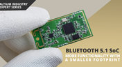
The list of features available in Bluetooth just got a little longer since the release of Bluetooth 5.1. If you want to incorporate a Bluetooth 5.1 SoC into your new product, you have two primary options for bringing this component into your board. The first is as an SoC that mounts to your board just like any other component. The other option is to bring a module into your new board—directly onto the surface layer. Here’s what you need to know about a Bluetooth 5.1 SoC or module in your next IoT product.
Blog
•
Altium 365 Getting Started User Guide - Available Now
Get Started with Altium 365 with a step-by-step guide and videos to experience the most connected experience for PCB design and realization: https://my.altium.com/altium-365/getting-started/

Blog
•
USB Power Delivery for Your Next Project
Since its introduction in the late 90s, the USB standard has never ceased to grow in popularity. There has been a growing trend toward USB being a power delivery interface with data, rather than a data interface that can supply power, as the 1.0 specification originally intended. To supply the increasing thirst for power over USB, the USB 3.0 Spec with Type-C began implementing the Power Delivery standard, which you should consider using for your next electronics project.
Blog
•
Circuit Board Design for In-Circuit Testing
There are many types of circuit board tests available in electronics manufacturing today, each having unique goals and characteristics. This article presents guidelines at the design level (schematic and layout) to enable the use of in-circuit testing (ICT) fixtures to verify proper component assembly. These simple test fixtures allow your board to be tested as its assembled, which helps identify and remove failed boards from your production run.
Blog
•
Planning for the Future with Cirris Systems and Altium
Technological advancements have been a hallmark of the past few decades, from the widespread adoption of internet technology to the smartphones and wireless devices we rely on every day to stay connected. Orlan Thatcher, Board Layout Specialist at Cirris Systems, could never have predicted the demand their services would generate. The company struggled with six different software platforms before switching to Altium Designer.

Blog
•
An Introduction to NFC
I used to work in a research lab that worked primarily with RFID (Radio Frequency IDentification) and NFC (Near Field Communication) technology, particularly for the agriculture industry and cattle identification. These were very specialized fields; however, the lab also worked on projects which involved retail and various other applications for NFC. It’s an amazing technology that you might be using every day without thinking about it - building access to your mobile phone payments, for instance.
Blog
•
Editing Your PCB Geometry with MCAD Tools
You need to define your PCB geometry in the context of your enclosure. If your board cannot physically be assembled into the final product, it doesn't matter how well laid out it is electrically. This webinar focuses on how the MCAD CoDesigner allows you to edit your PCB in the context of a higher-level assembly, allowing you to respect the relevant mechanical constraints.
Blog
•
The PCB Fabrication Process — what Every Design Engineer Needs To Know, Part 2
In Part 1 of this article, I described the first steps that occur during the PCB fabrication process. They detailed the inner layer processing effort as well as the efforts that take place during the transition from inner layer processing to lamination. This part of the article will provide a detailed description of the lamination, drilling and plating processes.
Blog
•
The PCB Fabrication Process—What Every Design Engineer Needs To Know, Part 1
There are still a number of designers - perhaps most of them - who have never toured a PCB fabrication facility. They are also unaware of the various steps that occur during the fabrication process. The purpose of this article is to describe those steps and what transpires in each of them. Part 1 of this article focuses on inner layer processing and the steps that are done prior the lamination process.
Blog
•
Webinar "8 Reasons to Store Your Components in Altium 365"
Working with local libraries seems like a simple solution, but we often don’t take into account the added time spent maintaining libraries and sharing them between team members. This webinar showcases the advantages of component storage in Аltium 365 to resolve the issues of local libraries and component management.

Blog
•
Bridging the Gap Between Designers and Customers
Every piece of electronic equipment starts with a great idea. Transforming great ideas into real, physical products takes a team of talented individuals and multiple companies coming together to make everything from the internal components to the external hardware. Paul Payen de la Garanderie, Founder and Owner of AW Audio, an engineering services company based in France, understands these challenges very well. With an extensive background in the Audio/Visual industry, Paul has had to work with multiple companies over the years, from small start-ups to celebrated AV firms.
















Your search returns no results.


