News & Updates

Blog
•
IPC-2221 Calculator for PCB Trace Current and Heating
The IPC-2221 standard includes many requirements for printed circuit board design and manufacturability, and there are several online calculators that have been developed based on this standard.


Blog
•
All About Box Build Assemblies
When you’re ready to manufacture a new device at production volume, there are many aspects of the product that must come together. The enclosure, cabling and connectors, embedded software/firmware, and of course the PCBA all have to be considered in totality. There is a quick way to get your product into a usable enclosure, complete with input power and cabling, and with a form factor that fits your PCBA. This overused route to a new product is a box build assembly.
Blog
•
Ultra-HDI Technology is Not New
Printed circuit board fabricators have become skilled at manufacturing these technologies and also at understanding the reliability and producibility challenges associated with high-density-interconnect technology. Let’s look at where the PCB industry is at today.



Blog
•
Today's PCB Designers Are Driving Electronics Product Design
What can the industry do to support PCB designers as they continue taking a more active role in product development? Here at Altium, there has been a progressive shift towards looking at the system level and creating tools that get designers more involved throughout the product development process. As the saying goes, over the wall engineering is over… today’s most successful products are built in a collaborative process.


Blog
•
Phased Array Antenna Design for 5G Applications
As the 5G rollout progresses and researchers continue to discuss 6G, many new 5G-capable products operating in sub-GHz and mmWave bands are reaching the marketplace. Devices that will include a 5G-compatible front-end, whether small stations/repeaters or handheld devices, use phased arrays as high-gain antenna systems to provide high data throughput without losing range at higher frequencies.


Blog
•
IPC - Vias
Via protection is an important part of modern PCB design. It provides additional benefits in PCB manufacturing and assembly, increasing the number of acceptable products.
Blog
•
Power Integrity Analysis in Your PCB Design Software
Power integrity problems can abound in modern PCBs, especially high-speed boards that run with fast edge rates. These systems require precise design of the PDN impedance to ensure stable power is always delivered throughout the system.



Blog
•
Schematic Compare
A design project doesn’t appear out of nowhere. The design process spreads over time, and project documents change. Schematic documents gradually become more complex, new functional blocks appear, and already finished parts can be modified and updated.

Blog
•
Embedded Capacitance Materials Overview
Capacitance is your friend whenever you need stable power integrity, which is why there is so much focus on decoupling capacitors. While these components are important and they can be used to provide targeted power integrity solutions to certain components, there is one specialty material used to supercharge capacitance in your PCB stackup or package substrate.
Blog
•
How To Import Libraries and Manage Components With Altium 365
The problems you can experience with components and libraries are endless. These problems are the most significant source of design issues and the biggest reason behind respins, costing companies untold amounts of lost profit annually.
If you want to have a better understanding of how to use Altium 365 to maintain a strong and centralized library that is free of problems and headaches, you may want to consider attending this lecture.

Blog
•
What's In Your BGA Land Pattern and Footprint
If you look in datasheets for most components, you’ll often find a recommended land pattern, usually alongside some mechanical package information and assembly information. This is not always the case with BGA components, especially components with high ball count. There are a few reasons for this that we can speculate: those ball counts might just be too big to put into a single page, or the manufacturer just expects you to know how to create that land pattern.
Blog
•
MIDs Make a Comeback as Vertical SMD Modules for Your PCB
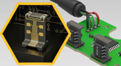
Molded interconnect devices are essentially plastic molded substrates with traces running along any surface, including at right angles and running vertically. Altium users can use the new 3D Routing extension to design their own component carriers, which can be mounted vertically in a standard assembly process. If you’ve always wanted to vertically mount components or entire circuits, but without the expense of adding a flex section to your design, the new 3D Routing extension with HARTING’s component carrier designs provides a unique solution.
Blog
•
MCAD CoDesigner 2.9.0 is Out
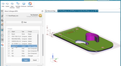
Altium has released version 2.9.0 of the MCAD CoDesigner. This version has the option to exclude small components when transferring from ECAD to MCAD. The arc behavior was improved, and the support for splines in board shape and cutouts was added. With this release, you can now select a specific SOLIDWORKS configuration of a part to use on the board and view the improvements made for Siemens NX.
Blog
•
Support for Rigid-Flex in Altium Designer
Altium Designer's world-class PCB design features help users quickly get started with new rigid-flex designs and prepare them for manufacturing. Rigid-flex in Altium Designer starts with designing a manufacturable PCB layer stack complete with via transitions and any calculated impedance requirements. Keep reading to see how Altium Designer supports your flex and rigid-flex designs.
Blog
•
2+N+2 PCB Stackup Design for HDI Boards
Like any other advanced PCB, success in HDI design comes from designing the right stackup. One common HDI stackup used to support routing into moderate pin count, high-density BGA components is the 2+N+2 PCB layer stack for HDI boards. We’ll explore this stackup more in this article, as well as how it is related to other advanced stackups used in HDI PCBs.
Blog
•
PDF in Altium 365 Web Viewer
Altium 365 Web Viewer now includes a built-in PDF viewer that allows you to view PDF files in releases without an external PDF viewer application. Keep reading to learn about new key features that make your work easier
Blog
•
Flex and Rigid-Flex PCB Applications
There are two basic reasons for designing a flex circuit into your product: to build a compact and efficiently assembled device, or to make the circuit dynamically integrated with the mechanical function of the product. You may, of course, lean on both of these reasons for justifying the use of flex circuits. On this note, let’s look at some rigid-flex PCB applications and design examples to see the issues that spring to mind when designing flex circuits
Blog
•
Granular Sharing — Role and Group Management
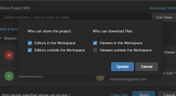
With Altium 365, you can grant permission to teams or users based on the specific needs of a project. We have expanded Altium 365’s file-sharing setting, giving you more granular control over who can download source files and reshare projects with others

Blog
•
Design Rule Checking in the PCB Design Workflow
Any time you design a PCB, and you want to turn it into a real product, you will have to make sure the design obeys the constraints within the standard PCB manufacturing process. This imposes multiple rules on any design, and ECAD software will enforce design rules as you create the board to ensure you obey these important constraints. Make sure you enforce the right design rules at the beginning of the PCB design workflow
Blog
•
Best Practices for High-Frequency PCB Material Selection
High frequency PCB design can seem esoteric, and I've heard many an engineer describe it as "black magic"! The subject is also a bit confusing, especially once someone asks which frequencies could be reasonably considered "high". Before you do anything inside the layout for a high-speed or RF PCB, you will need to pay attention to the materials being used in the board. If you're unsure which high frequency PCB materials you should use, then keep reading to learn more.

Blog
•
PCB Noise Reduction: Do You Need Isolation, Shielding, or Filters?
Of all the noise and operational challenges designers face in their PCBs, there is one overarching problem that is arguably most popular: electronic noise. It could originate as an SI/PI problem, it could possibly arise from some external source, or it could be good old-fashioned crosstalk! These tend to fall into three categories: adding shielding, doing something to create isolation, or placing filters. Let's look at all of these as they tend to be the default solution set when confronted with many noise problems.
Blog
•
What’s New in Altium 365: Version Control for Hardware, Layer Stackup in Web Viewer, and SOC 2 Type 1 Certification
In February, we hit a new record in the number of users on the platform. The Altium 365 user community is now 20,000 strong! You can now migrate from an external version control system to Altium 365 preserving the history of commits. We also received the SOC 2 Type 1 certification from KPMG, made layer stack available in the web viewer, and added the brand new capability to track tasks in the context of your design project. Keep reading to learn more!

Blog
•
Introducing Spectra's Electronic Design to Delivery Index
Get a cohesive view of supply chain market conditions, stay on top of trends, and avoid disruption with this free, monthly report from Spectra.
Blog
•
Support for Rigid-Flex in Altium Designer
Rigid-flex in Altium Designer starts with designing a manufacturable PCB layer stack complete with via transitions and any calculated impedance requirements. Flex sections also need to be placed in the layer stack before moving into the PCB layout. Once inside the PCB editor, bending lines can be clearly defined in the PCB layout, and these can be visualized in Altium Designer's 3D PCB design tools. Keep reading to see how Altium Designer supports your flex and rigid-flex designs.
Blog
•
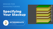
Communicating PCB Layer Stackup Needs to Manufacturers
In the business of PCB design, communicating needs to manufacturers and vendors is a top priority. The context of our requests is sometimes lost either by not providing the correct information, not listing enough information, or not giving any information. Although the experienced PCB designer can take steps to specify everything they want to see in their PCB stackup, eventaully the manufacturer will handle that decision in an effort to balance available materials with processing capabilities and yield.
Blog
•
Risk Vs. Reward
During the recent IPC APEX expo, there was a lot of discussion about SAP, or semi-additive PCB processes. As with any new technology adoption there were people that are excited to jump right in and start designing with much finer feature sizes and work through the inevitable changes to the traditional thought process. Others are in a "let’s wait and see" mode and of course there are a few skeptics there as well, so keep reading to learn more.






Your search returns no results.


