News & Updates


Blog
•
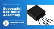
All About Box Build Assemblies
When you’re ready to manufacture a new device at production volume, there are many aspects of the product that must come together. The enclosure, cabling and connectors, embedded software/firmware, and of course the PCBA all have to be considered in totality. There is a quick way to get your product into a usable enclosure, complete with input power and cabling, and with a form factor that fits your PCBA. This overused route to a new product is a box build assembly.
Blog
•
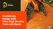
Ultra-HDI Technology is Not New
Printed circuit board fabricators have become skilled at manufacturing these technologies and also at understanding the reliability and producibility challenges associated with high-density-interconnect technology. Let’s look at where the PCB industry is at today.


Blog
•
Today's PCB Designers Are Driving Electronics Product Design
What can the industry do to support PCB designers as they continue taking a more active role in product development? Here at Altium, there has been a progressive shift towards looking at the system level and creating tools that get designers more involved throughout the product development process. As the saying goes, over the wall engineering is over… today’s most successful products are built in a collaborative process.


Blog
•
Phased Array Antenna Design for 5G Applications
As the 5G rollout progresses and researchers continue to discuss 6G, many new 5G-capable products operating in sub-GHz and mmWave bands are reaching the marketplace. Devices that will include a 5G-compatible front-end, whether small stations/repeaters or handheld devices, use phased arrays as high-gain antenna systems to provide high data throughput without losing range at higher frequencies.


Blog
•
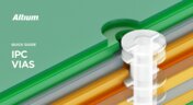
IPC - Vias
Via protection is an important part of modern PCB design. It provides additional benefits in PCB manufacturing and assembly, increasing the number of acceptable products.
Blog
•
Power Integrity Analysis in Your PCB Design Software
Power integrity problems can abound in modern PCBs, especially high-speed boards that run with fast edge rates. These systems require precise design of the PDN impedance to ensure stable power is always delivered throughout the system.



Blog
•
Schematic Compare
A design project doesn’t appear out of nowhere. The design process spreads over time, and project documents change. Schematic documents gradually become more complex, new functional blocks appear, and already finished parts can be modified and updated.

Blog
•
Embedded Capacitance Materials Overview
Capacitance is your friend whenever you need stable power integrity, which is why there is so much focus on decoupling capacitors. While these components are important and they can be used to provide targeted power integrity solutions to certain components, there is one specialty material used to supercharge capacitance in your PCB stackup or package substrate.
Blog
•
How To Import Libraries and Manage Components With Altium 365
The problems you can experience with components and libraries are endless. These problems are the most significant source of design issues and the biggest reason behind respins, costing companies untold amounts of lost profit annually.
If you want to have a better understanding of how to use Altium 365 to maintain a strong and centralized library that is free of problems and headaches, you may want to consider attending this lecture.

Blog
•
Unveiling the Crucial Role of PCB Harness Design Capabilities in Multi-Board Designs
Multi-board designs are the key to meeting evolving demands, requiring robust PCB Harness Design for seamless interconnection and success. Join us as we explore the importance of PCB Harness Design capabilities and how they are crucial for the success of multi-board designs.
Blog
•
What Makes a PCB Enclosure Rugged?
Whether you purchase products off-the-shelf or online, they all come housed within an enclosure. In some cases, these enclosures are intentionally ruggedized to withstand harsh environments or mechanical shocks. You can learn more about enclosures in this new and interesting article.
Blog
•
Concept Phase – Lid Assembly Design Part 2
We are continuing our journey through the lid assembly design phase of our Open Source Laptop project. In this section, we will discuss the layout of the test adapter and provide a demonstration of the first test for the display panel, along with the initial steps involved in assembling the boards.
Blog
•
Concept Phase – Lid Assembly Design Part 1
In the exciting next phase of the open-source laptop project we're (finally) diving into design, and getting hands-on with the display panel. Discover how we're selecting the right panel, integrating it seamlessly, and creating a custom DisplayPort adapter to illuminate the screen. Plus, learn how our choices impact features like microphones, webcams, and touch sensors, and how Altium can help bring it all to life. It’s not too late to join as we continue on this innovative journey!
Blog
•
Unleashing the Power of Concurrent PCB Design
Concurrent PCB Design is essential to unlocking the full potential of engineering teams and delivering innovative products that meet the demands of the modern world. Learn more about the main capabilities and the numerous benefits of this upcoming feature in Altium Designer.

Blog
•
Crosstalk Reduction and Elimination Techniques in Altium Designer
Whether you're designing a digital board with a ton of traces, or an RF board operating at very high frequencies, any electronic device with propagating signals will experience crosstalk. Learn more about some sure-fire ways you can reduce crosstalk in your high-speed designs.

Blog
•
Baxandall Volume Control for Audio
The Baxandall volume control is an especially useful, flexible, and simple-to-implement circuit for numerous audio designs. In this article, we will demonstrate how to design this type of equipment.

Blog
•
Common Flex Design Mistakes and How to Fix Them
Designing flexible circuits involves managing numerous factors. Discover how to prevent mistakes in this process and how to rectify them post-implementation.
Blog
•
How Much PCB Mask Expansion is Too Much?
In this article you will learn about finding the right balance between PCB mask expansion and potential problems.
Blog
•
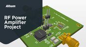
RF Power Amplifier Module PCB Design
RF power amplifiers can be found in many wireless products, often integrated into chipsets or modems. However, in certain specialized systems, you might require higher power output at a specific frequency. This necessitates a discrete amplifier circuit to deliver that power. In this article, we present an example project for a power amplifier that you can incorporate into your RF project.

Blog
•
Avoid GIGO in Your PCB Simulation Tools
Simulation tools are extremely useful for understanding electromagnetic behavior in a design. Learn more about how to avoid obtaining inaccurate results during your PCB simulation process.
Blog
•
Choosing a Converter or Regulator For Your Power Supply Design
When designing the power supply for your device, there are lots of different options. In this article, we will take a brief tour of the main choices in DC power supply design.

Blog
•
The Benefits of Ultra HDI
Learn more about the combination of using both flexible materials and ultra-HDI feature sizes in this article.
Blog
•
Understanding Power Supply Current Handling Issues: Causes and Solutions
Troubleshooting power supply current handling issues is crucial to achieving optimal performance of your electronic devices. In this article, we will explore the common reasons why a power supply fails to handle the defined output current and provide practical solutions to solving these issues.
Blog
•
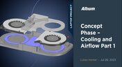
Concept Phase – Cooling and Airflow Part 1
Next step in our open-source laptop project is to explain how to design cooling and airflow. In this article, we can show you the first part of this process, such as airflow concept, fan measurement and clearance.
Blog
•
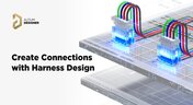
Create Connections with Harness Design
Many modern electronics have multiple boards, and connecting those different boards and systems together are harnesses. Learn more about how Altium Designer can help you create harnesses for your own multi-board designs here.















Your search returns no results.


