Welcome, Guest

Sign in to learn, create, and do more with the product you love.

News & Updates

Filters:
Tag
Embedded thumbnail for Polygon Pours
Working with Polygons
Polygon Pours

Polygon pours are used to create copper geometries on your board. You can prioritize polygon pour order, hide them to make it easier to work on your board, and repour them to resolve design rule conflicts.

Embedded thumbnail for How to Use the MCAD CoDesigner?
How-To's
How to Use the MCAD CoDesigner?

This video shows how the ECAD and MCAD engineers now can communicate directly while staying within their own design environment. The MCAD engineer is able to push design information directly from their design software straight into Altium Designer. Any changes can be reviewed, accepted, or denied by the receiving party. This process of pushing and reviewing design changes is bi-directional, meaning that both the MCAD or ECAD engineer can push and review changes to the other. 

chip with neon illumination
Blog
How Does the Package PDN Impact Power Integrity?

Whenever we say something to the effect of “components can’t work without a correctly designed PCB,” we only have to look at component packaging for evidence. It is true that component packages come with parasitics that affect signal integrity, but there is one area that we don’t often look at in terms of component packaging: power integrity.

Embedded thumbnail for Creating Additional Snap Points Using a 3D Model
How to use Snapping
Creating Additional Snap Points Using a 3D Model

Demonstration of using snap points with 3D models and how they can assist in the placement of said models.

electrical circuit with microcontroller
Blog
Designing Custom Hardware with Microcontrollers

In this article, we’ll look at all that is required to start creating your own custom microcontroller-based hardware designs. You’ll see that there actually isn’t too much to this, as microcontroller manufacturers over the years have tried to make the learning curve less steep and their devices more, and more accessible. This is both from an electrical point of view but also – equally importantly – from a programming point of view.

Embedded thumbnail for Polygon Connect Styles
Working with Polygons
Polygon Connect Styles

Define how vias and pads connect to polygons with a design rule. Customize the thermal relief width, number, and rotation as well as the air gap width.

Embedded thumbnail for How to work with Component Classes?
How to Work with Classes
How to work with Component Classes?

Modern printed circuit boards can contain a large number of components, which makes them difficult to work with. In this video we will show what component classes can be on a PCB, how to create custom component classes and how they can be useful for us. 

high-speed printed circuit board
Blog
Guide to Low-Dk PCB Materials

If you’ve taken time to learn about PCB material options and layer constructions, you have probably seen the wide range of materials that are available on the market. Materials companies produce laminates with varying Dk values, Tg values, weave styles, CTI values, and mechanical properties to target various applications in the electronics industry.

printed circuit board, photo by the author
On-Demand Webinar
Learn to Collaborate Like a Pro with Altium Designer 23

Get ready to speed up your design process with new Altium Designer collaboration capabilities. Designing a PCB is a team effort. Engineers must work with customers, manufacturers, and other stakeholders to get the best results. You need help to bring your design to life, even if you're a one-person team.

freeway in the background of the city
Blog
Designing for V2X Communication: Wireless Protocols and Standards

If you’re waiting for truly connected cars on a grand scale, there is still a massive amount of work to be done, both on the hardware and software sides. Connected cars can only become a widespread reality once the automotive industry and telecom carriers can decide which protocol will work best for vehicle-to-everything (V2X) communication. PCB designers will then need to step in to create these systems and fit them into a vehicular environment.

Embedded thumbnail for Create and Snap to a Circular Grid (Polar Grid)
How to use Snapping
Create and Snap to a Circular Grid (Polar Grid)

Instructional on how to create polar grids, how to snap to them, and why you might want to use them.

Embedded thumbnail for How to Connect Polygons to Nets
Working with Polygons
How to Connect Polygons to Nets

This video covers how to easily connect a polygon to a net using just two clicks. With the Properties panel open and a polygon selected, click the "Assign net" button in the Properties panel.

Embedded thumbnail for Altium 365 Getting Started: Gerber Compare
Getting Started with A365
Altium 365 Getting Started: Gerber Compare

The task of comparing different versions of manufacturing files usually arises when the electrical engineer needs to check and confirm the manufacturer's edits or clarify details of changes before starting production. In Altium 365 you can perform an automatic comparison of Gerber files. 

Embedded thumbnail for Altium 365 Getting Started: Migrate to Altium 365 from other VCS
Getting Started with A365
Altium 365 Getting Started: Migrate to Altium 365 from other VCS

The development of electronic devices always involves the release of many different types of files. And these files are not static - they change as the project progresses. Traditionally, one way to manage data is to use a version control system such as Git or SVN. Unlike other VCSs, Altium 365 is the system designed specifically for managing project data.

Everything You Need to Know About Stitching Vias
Blog
Everything You Need to Know About Stitching Vias

This one area of PCB design can be contentious among some designers as it is related to copper pour, which it is often stated is not needed in most designs. Regardless of your feelings about copper pour, stitching vias have important uses in PCBs at low frequencies and at high frequencies.


Embedded thumbnail for How to get a BOM for a Multi-board Design
How-To's
How to get a BOM for a Multi-board Design

When designing a multi-board project, an up-to-date and accurate BOM for the entire device is a necessity. Watch this video to learn how to properly create a BOM for your multi-board project.

Embedded thumbnail for Remove Unused Pad Shapes
Working with Polygons
Remove Unused Pad Shapes

Unused pad shapes create holes in your copper geometries. You can quickly examine all pads in the design to remove unused pad shapes and restore previously removed pads. 

Embedded thumbnail for Effective use of "Objects for snapping" when creating a Footprint
How to use Snapping
Effective use of "Objects for snapping" when creating a Footprint

Learn how to effectively use snaps that allow you to create a component footprint quickly and conveniently

Tag
Harness Design
Blog
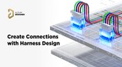
Create Connections with Harness Design

Many modern electronics have multiple boards, and connecting those different boards and systems together are harnesses. Learn more about how Altium Designer can help you create harnesses for your own multi-board designs here.

Blog
Nucleo Shields Multi-Board Design

Learn how easy it is to create multi-board projects. This practical project article covers the reasons for breaking larger boards into sub-assemblies and explores the various connection options available between sub-assembly boards.

Blog
Analog Solar Tracker Project

In this article you can learn about light sensors while building an analog solar panel tracking system. This open-source project covers multi-channel design, window comparators, driving motors, and photosensors.

Blog
Concept Phase – Initial CAD Design

We are continuing our journey through the open-source laptop project. This article explains an initialization of CAD design process from the early concept and brainstorming phase.

Blog
High-Speed PCB Design Tips

Essential tips for high-speed PCB designs, and when you need to start being concerned about how and where you route your traces.

Introduction to Open Source Laptop Project
Blog
Introduction to Open Source Laptop Project

We have started a very exciting journey into the creation of an open source laptop project. This project will be an ongoing one, with our community able interactively participate. By utilizing Altium 365 users will be able to view, comment on, and download design files. This will be a great learning experience for new and experienced PCB designers.

Blog
Ebook: Routing High-Density Interconnects with Reliable Microvias

HDI PCBs take a particular approach to routing interconnects through multiple layers to ensure reliability during fabrication, assembly, and operation. The critical structure that enables this is microvias, which are prone to failure if not designed properly. In this e-book, readers will receive an initial look at the reasons microvia reliability has come into the spotlight and why HDI PCB designers put reliability first when routing through microvias.

Blog
IPC-2221 Calculator for PCB Trace Current and Heating

Aside from impedance and annular ring calculations, one of the other major formulas specified in the IPC 2221 standard relates temperature rise, trace width, and trace current. THere is also the IPC-2152 standard, both include this guidance on designing for thermal reliability, but which standard should we use?

Blog
Stripline Impedance Calculator

Striplines provide some advantages over microstrips as they take advantage of natural shielding and coupling from nearby ground plane layers. Although they tend to experience higher losses due to total confinement in the dielectric, they can be thinner due to the high dielectric constant used in internal layers of a PCB. Use our free impedence calculator to help you determine the correct width needed to hit a target impedance.

Blog
Which Types of Opto-Isolators Are Right For Your Signal?

An optoisolator is a cool electronic device that can be used to pass information between a diode without passing an electrical current. There are many great applications for these, but do you know which one is right for you?

Tag
Embedded thumbnail for Cross Select Mode
How to work with Selection
Cross Select Mode

Cross Select Mode is a unique tool that allows for cross-selection of objects between the schematic and PCB thanks to the Altium Unified platform. This makes it easy to look for specific components, as well as take advantage of component placement tools.

Embedded thumbnail for Tools for Efficient Selection
How to work with Selection
Tools for Efficient Selection

Efficient selection tools can make a difference in how long and how clean your design can be. Learn how to utilize the Edit Select Menu tools in Altium Designer to take control over your layout.

Embedded thumbnail for Tools for Easily Selecting Objects in the PCB
How to work with Selection
Tools for Easily Selecting Objects in the PCB

Explore more than basic mouse movements by taking a look at the tools that Altium Designer has to offer for making selecting and moving objects in the PCB an easy task. This will increase your productivity and allow you to spend more time designing

Embedded thumbnail for How to Work with The Polygon Manager
Working with Polygons
How to Work with The Polygon Manager

It is important to have a high-level view of all polygons on the PCB design. The Polygon Manager lets you rename polygons, set their pour order, perform re-pouring or disable pouring on selected polygons, add/scope the polygon connection style and clearance design rules, and add polygon classes for selected polygons.

Embedded thumbnail for Assigning Impedance Profiles for Differential Pairs
How to Work with Differential Pairs
Assigning Impedance Profiles for Differential Pairs

When you assign an impedance profile to a differential pair you open up several options for control over your routes. We'll show you how to do just that, as well as how to fix errors that may pop up and how to create classes for differential pairs based on assigned impedance profiles.

Embedded thumbnail for How to Highlight or Select Net Connections in the PCB
How-To's
How to Highlight or Select Net Connections in the PCB

We’ll show you how to highlight net selections so you can easily track where connections are made. We’ll show you how to hide and show nets, and how to use the view configuration and PCB panels to view and highlight nets across your design, and how to assign net colors in both the PCB and the schematic.

Embedded thumbnail for Remove Unused Via Pads
How to Design a BGA
Remove Unused Via Pads

The Remove Unused Pad Shapes tool in Altium Designer gives you control over the via pads in your design. We’ll show you how to use it to increase the usable area of power and ground polygons, increase the density of conductors between hole rows, and fixing incorrect connections.

Embedded thumbnail for Tent Vias under BGA
How to Design a BGA
Tent Vias under BGA

When via are located close to component pads some soldering issues can arise, but this can be fixed with Tented vias. We’ll show you how to manually tent vias and how to tent vias through the Design Rules.

Embedded thumbnail for Via-in-Pad for BGA
How to Design a BGA
Via-in-Pad for BGA

We’ll teach you how to use Via-in-pad to reduce inductance, improve signal integrity, and improve power distribution system performance in BGA designs.

Embedded thumbnail for Using HDI Stackups during BGA Design
How to Design a BGA
Using HDI Stackups during BGA Design

Micro Vias and Buried Vias play an important role in high density interconnection layer stackups (HDI Stackups). We’ll show you how to add via and create rules to allow you to take full advantage of the HDI Stackup.

Embedded thumbnail for Automatic Fanout With BGA
How to Design a BGA
Automatic Fanout With BGA

When routing a BGA it can be necessary to use automatic fanout to make the routing process easier and faster. We’ll show you how to run the automatic fanout for routing a BGA and how the rules can affect the outcome of the route.

Embedded thumbnail for Specifying NSMD and SMD for BGA
How to Design a BGA
Specifying NSMD and SMD for BGA

BGA layouts use two types of pads: SMD, Solder Mask Pads, or NSMD, Non-Solder Mask Pads. Here we’ll walk you through the differences and how to specify and edit them for your layout.

Embedded thumbnail for Via Shielding and Stitching
Via Stitching
Via Shielding and Stitching

Altium Designer gives you full control over your via shielding and stitching. We’ll show you how to use our shielding and stitching tools, how to alter their parameters, and how to remove any unwanted via shielding and stitching.

Embedded thumbnail for xSignals for DDR3 and DDR4
How To Work with High-Speed Projects
xSignals for DDR3 and DDR4

In a high-speed design, DDR3 and DDR4 memory chips can utilize xSignal classes to match track lengths from the controller to the memory chip easily and quickly using the xSignals wizard.

Embedded thumbnail for High-Speed Tuning
How To Work with High-Speed Projects
High-Speed Tuning

If you use high-speed interfaces like USB 3.0, PCIE, or DDR3/DDR4, you need to use match length tuning to ensure that they work properly. We’ll show you why and how, as well as demonstrating the different tools for length tuning.

Embedded thumbnail for Using Document Parameters with Draftsman
How to Work with Draftsman
Using Document Parameters with Draftsman

The Draftsman Editor in Altium Designer uses document parameters to allow fine grain control over the draftsman document. We’ll show you how you can use the document parameters in your Draftsman document. 

Tag
Your search returns no results.