Welcome, Guest

Sign in to learn, create, and do more with the product you love.

News & Updates

Filters:
Tag
Embedded thumbnail for PCB Classes overview
How-To's
PCB Classes overview

Are there too many primitives on the board? Having trouble creating design rules? This video gives a brief overview of the classes of primitives that can be created on the board, as well as the possibilities for their further use.

Blog
Ebook: Routing High-Density Interconnects with Reliable Microvias

HDI PCBs take a particular approach to routing interconnects through multiple layers to ensure reliability during fabrication, assembly, and operation. The critical structure that enables this is microvias, which are prone to failure if not designed properly. In this e-book, readers will receive an initial look at the reasons microvia reliability has come into the spotlight and why HDI PCB designers put reliability first when routing through microvias.

Embedded thumbnail for Creating a BGA Footprint with the Footprint Wizard
How-To's
Creating a BGA Footprint with the Footprint Wizard

Altium Designer makes it easy to create a BGA footprint using our IPC compliant footprint wizard. We'll show you how easily you can create and modify a BGA footprint using the footprint wizard.

Blog
IPC-2221 Calculator for PCB Trace Current and Heating

Aside from impedance and annular ring calculations, one of the other major formulas specified in the IPC 2221 standard relates temperature rise, trace width, and trace current. THere is also the IPC-2152 standard, both include this guidance on designing for thermal reliability, but which standard should we use?

Embedded thumbnail for How to work with Pad Classes on PCB?
How-To's
How to work with Pad Classes on PCB?

Sometimes it is required to set different design rules for a different set of pads on the board. The easiest way is to use pad classes and in this video we'll show you how easy it is to create and apply them.

Embedded thumbnail for How to work with multivariate calculations?
How-To's
How to work with multivariate calculations?

Additional modes for obtaining temperature, parametric dependencies and probabilistic distribution by the Monte Carlo method are performed together with basic calculations and allow expanding the possibilities for analyzing design results.

Embedded thumbnail for How to calculate Transient Analysis?
How-To's
How to calculate Transient Analysis?

Transient Analysis simulates the reaction of a circuit over a period of time. It can be supplemented by Fourier Analysis and the use of Initial Conditions.

Embedded thumbnail for BOM Comments
How-To's
BOM Comments

Convenient interaction and coordination of the Active BOM with the help of comments is possible both from the web version of the project and from the Altium Designer between participants of the same and different roles.

Blog
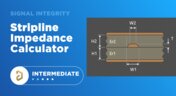
Stripline Impedance Calculator

Striplines provide some advantages over microstrips as they take advantage of natural shielding and coupling from nearby ground plane layers. Although they tend to experience higher losses due to total confinement in the dielectric, they can be thinner due to the high dielectric constant used in internal layers of a PCB. Use our free impedence calculator to help you determine the correct width needed to hit a target impedance.

Embedded thumbnail for Query Language: What is It For?
How-To's
Query Language: What is It For?

A PCB project contains many different objects. How to manage them? How to find the right ones quickly and efficiently? This video starts the series about query language. Learn the language commands and how to use them and expand your possibilities!

Blog
Which Types of Opto-Isolators Are Right For Your Signal?

An optoisolator is a cool electronic device that can be used to pass information between a diode without passing an electrical current. There are many great applications for these, but do you know which one is right for you?
Blog
Properties panel document options in SCH editors

The Properties panel provides access to the properties of documents and objects. The contents of the panel change depending on the active document or the selected object. This blog will quickly go over some of need to know options around the properties panel in the schematic document.

Embedded thumbnail for PCB design with BGA: Via-in-Pad
How-To's
PCB design with BGA: Via-in-Pad

We’ll teach you how to use Via-in-pad to reduce inductance, improve signal integrity, and improve power distribution system performance.

Embedded thumbnail for Design RF PCB: Distributed-Element Circuits
How-To's
Design RF PCB: Distributed-Element Circuits

Distributed-element circuits are a topology of a particular shape and size. Filters, power dividers, directional couplers can be built from them. Being calculated in third-party CAD, the topology of such elements can be easily imported into Altium Designer, and we will show you how to do it!

Embedded thumbnail for How to work with components on a rigid-flex board in MCAD
How-To's
How to work with components on a rigid-flex board in MCAD

With MCAD Codesigner you can quickly add and move components from your MCAD tool and update the design automatically in Altium Designer. We’ll show you how to. Add a new component, move components, and change a component’s region in MCAD, and update it to your design in Altium Designer.

Embedded thumbnail for LSM: Impedance profile
How-To's
LSM: Impedance profile

Creating Impedance profiles for transmission lines and how to apply them to the board

High-Speed PCB Stackup Design
Blog
The High-Speed PCB Stackup Design Challenge

Even with all the good guidelines out there for high speed design, there are particular aspects of stackup construction and their relation to building boards that get overlooked. This blog is goes beyond just the typical SI/PI guidelines and looks at these problems from more of an engineering perspective.

Embedded thumbnail for Multichannel Schematic: Creating Channels
How-To's
Multichannel Schematic: Creating Channels

Altium Designer makes creating single and multichannel designs effective and quick. We’ll show you how to create and annotate output and input channels in your design.

Embedded thumbnail for How to efficiently use Blankets?
How-To's
How to efficiently use Blankets?

Blanket is a powerful tool for group assignment of properties in schematic documents. It makes it easier and faster to assign circuit classes, differential pairs, and design rules within schematic documents. This video provides instructions on how to use blanket to simplify work in your designs.

stitching vias
Blog
Everything You Need to Know About Stitching Vias

Stitching vias are something you often see spread around the surface layer of a PCB, but what are they? and should you be using them? In this guide, we'll go over some of the standard uses of stitching vias and when they should be used in a PCB.

Tag
Article preview
Blog
Webinar "8 Reasons to Store Your Components in Altium 365"

Working with local libraries seems like a simple solution, but we often don’t take into account the added time spent maintaining libraries and sharing them between team members. This webinar showcases the advantages of component storage in Аltium 365 to resolve the issues of local libraries and component management.

Article preview
Blog
Bridging the Gap Between Designers and Customers

Every piece of electronic equipment starts with a great idea. Transforming great ideas into real, physical products takes a team of talented individuals and multiple companies coming together to make everything from the internal components to the external hardware. Paul Payen de la Garanderie, Founder and Owner of AW Audio, an engineering services company based in France, understands these challenges very well. With an extensive background in the Audio/Visual industry, Paul has had to work with multiple companies over the years, from small start-ups to celebrated AV firms.

Blog
Additive PCB Manufacturing: The Vaccine for Electronics Supply Shocks?

At this time, at least a quarter of the world’s population is under quarantine, with workers unable to go to offices or factories, leading to fundamental disabling of the world economy. The electronics industry is suffering greatly as well, dealing with a supply shock from factories shutting down in Southeast Asia, to demand-side shocks from Western markets literally shutting down. Now it is the electrical engineers taking the lead with additive PCB manufacturing.
Article preview
Blog
Webinar "6 Steps to Master Project Storage"

Altium 365 provides a secure cloud platform to store all of your design files in a single place so you can share them with anyone and access them from anywhere. This webinar discusses the advantages of placing, storing, and working with projects in Altium 365.


Article preview
Blog
Altium Designer 20 Changed My Layout Design Routines

I just finalized my first PCB design using Altium Designer 20. At the same time, I tested some new AD20 features, and in this article, I’ll share my thoughts about new layout design features which made the biggest impression for me: sliding, and any-angle routing.

Article preview
Blog
Designing for Antenna Isolation in Your Wireless System

Anyone who has taken apart an old cell phone or designs IoT devices knows multiple communication capabilities are present in these designs, each requiring different antennas. The RF designer should already take precautions for interconnect isolation, but antenna isolation is just as important when modeling and designing wireless systems.

Blog
PCB Trace and Pad Clearance: Low vs. High Voltage

High voltage/high current designs carry safety requirements which need to be met by designers. Similarly, high speed designs need to have suppressed crosstalk in order to ensure signal integrity. The key design aspects that relate to both areas are your PCB trace clearance and pad clearance values. These design choices are critical for balancing safety, noise suppression, and manufacturability.

Blog
Getting Through PCB DFM

In this article, we’ll discuss the key design features to implement, and steps to take prior to fabrication that will help prevent some DFM process pain.

Altium Designer Getting Started User Guide
Blog
Level Up Your Design Skills - Altium Designer Getting Started User Guide Update
We are happy to announce the new update of our Altium Designer Getting Started User Guide. Whether you are new to Altium Designer or you want to brush up on some topics, the Altium Designer Getting Started User Guide will take you from a beginner to a master in PCB design.  This is only the beginning! This guide will be updated with new information based on user feedback. Let’s first go over the contents of the guide.
Article preview
Blog
Modeling Copper Foil Roughness in Altium Designer's Impedance Profiler

With the new layer stack manager in Altium Designer®, you can now include copper foil roughness factors directly in your impedance calculator. This is quite easy to do in the layer stack manager, but it begs the question: what exactly is the copper roughness factor? Which value should be used for your interconnects?

Article preview
Blog
High-Speed Signal Routing: The 5 Important Constraints

After you capture your schematic as an initial layout and create an initial component arrangement, it’s time to define your routing constraints. Doing this early will allow your DRC engine to spot rules violations before you finish your layout. Likewise, you’ll be able to modify the default rule set to meet your layout requirements. Here are the important routing constraints you’ll need to check before you start routing your board.

Blog
How to Create a PCB Manufacturing Cost Estimation

Some manufacturers have very convenient PCB manufacturing cost estimation calculators you can use, but the real costs depend on a number of factors. If you’re an entrepreneur and you’re producing your own boards, or you are managing manufacturing, testing, and delivery for a new project, it’s your job to help clients understand the primary cost drivers for new boards. Here’s how you can get an estimate of your fabrication costs, both for local and overseas manufacturers.

Blog
PCB Mountable Connectors: SMD vs. Through-hole

Selecting a connector is as much an art as it is a science. The artistic side is all about aesthetics and satisfying clearances, while the scientific side is all about signal integrity. For PCB mountable connectors, you’ll need to choose between surface-mounted or through-hole connectors, and you’ll need to consider how each type affects signal integrity in your application. Here’s what you need to think about beyond the standard connector specifications.

Article preview
Blog
PCB Via Current-Carrying Capacity: How Hot is Too Hot?

Trace and via current-carrying capacity are legitimate design points to focus on when designing a new board that will carry high current. The goal is to keep conductor temperatures below some appropriate limit, which then helps keep components on the board cool.

Blog
How to Maximize Copper in Your PCB Design: The Pros and Cons of Copper Pouring Versus Placing

There is a saying in copper pour PCB design, “Copper is free.” It means a PCB editor designer must think in reverse. A board starts off as solid copper, and the copper you don’t want is removed. It is faster to build, less consumptive, and less expensive to make a board that is mostly copper as compared to the same size board that is mostly bare. Picking the correct technique will make the difference between an effortless or frustrating experience.

Tag
NEW
Embedded thumbnail for Create Clearance Rules Faster and with Less Effort
New in Altium's Software
Create Clearance Rules Faster and with Less Effort

Setting up clearance rules is now more intuitive in the Constraint Manager. Choose the Simple view for faster configuration with grouped object types, or the Advanced view when you need detailed, matrix-based clearance control.

NEW
Embedded thumbnail for Mastering HDI Design Rules in Altium Designer
How-To's
Mastering HDI Design Rules in Altium Designer

In our latest Altium Academy tutorial, we guide you through configuring the essential HDI PCB design rules in Altium's software. You'll learn how to use your manufacturer's fabrication capabilities to create accurate design rules and constraints for your PCB.

Embedded thumbnail for Search, Filter, and Navigate PCB Designs Faster
New in Altium's Software
Search, Filter, and Navigate PCB Designs Faster

The Web Viewer now features a redesigned search experience for faster access to PCB design data across supported CAD formats. A lightweight, intuitive interface lets you begin with simple search terms and progressively refine results using contextual suggestions.

Embedded thumbnail for Gain Better Control Over Wire Bond Visibility
New in Altium's Software
Gain Better Control Over Wire Bond Visibility

New bond wire visibility controls give you greater flexibility when working with wire-bonded boards and footprints, making it easier to focus on the details that matter most.

Embedded thumbnail for Coming Soon: Selectable Harness Source Within Multi-board Design
New in Altium's Software
Coming Soon: Selectable Harness Source Within Multi-board Design

Selectable Harness Source Within Multi-board Design enables harness projects to drive system connectivity while maintaining bidirectional synchronization between multi-board schematics and harness wiring diagrams for improved accuracy and easier design management.

Embedded thumbnail for Choose the Simbeor Version for Your PCB Calculations
New in Altium's Software
Choose the Simbeor Version for Your PCB Calculations

The PCB Editor now lets you choose the Simbeor version used for delay and impedance calculations, giving you more flexibility and consistency across your design workflows.

Embedded thumbnail for Improve PCB Editor Performance with Via Instancing
New in Altium's Software
Improve PCB Editor Performance with Via Instancing

The PCB Editor now uses via instancing to generate geometry for each via individually, providing greater flexibility and a more advanced approach to managing vias in PCB designs.

Embedded thumbnail for GSSG Stackup Deep Dive: Routing, Impedance, and HDI
How-To's
GSSG Stackup Deep Dive: Routing, Impedance, and HDI

A ground-signal-signal-ground (GSSG) stackup rethinks the traditional four-layer PCB structure by moving the ground planes to the outer layers and routing signals on the two inner layers. In this Altium Academy deep dive, we review a real one-minute design review submission and demonstrate how to configure a GSSG stackup properly using the Layer Stack Manager.

Embedded thumbnail for Generate IPC-7351B Compliant Footprints with More Control
New in Altium's Software
Generate IPC-7351B Compliant Footprints with More Control

The IPC Compliant Footprint Wizard has been updated to improve IPC-7351B compliance across supported package types. Enhancements include footprint calculations, package outlines, silkscreen and courtyard generation, layer mapping, density table behavior, and new pad trimming controls for gullwing packages, with support added to the batch generator Excel template.

Embedded thumbnail for Add Unit-Aware Temperature Coefficient Parameters
New in Altium's Software
Add Unit-Aware Temperature Coefficient Parameters

Component templates in a connected Workspace on the Altium Platform now include support for Temperature Coefficient (ppm/°C) as a unit-aware user parameter type. This makes it possible to define temperature coefficient values directly within the template using the appropriate units.

Embedded thumbnail for When to Add Part Numbers to SMD Passives
How-To's
When to Add Part Numbers to SMD Passives

Check out our new video covering essential electronics fundamentals, with a focus on why including part numbers for SMD passive components, such as SMD resistors, directly on schematics is so important. We also explore whether relying only on the Bill of Materials (BOM) is enough for effective electronic component management.

Embedded thumbnail for Present Large Harness Tables More Clearly
New in Altium's Software
Present Large Harness Tables More Clearly

Harness Draftsman now supports splitting connection tables across multiple pages in *.HarDwf documents. With the new page height limit setting, you can easily control how much of the table appears on each page.

Embedded thumbnail for Innovate Beyond - The Future of Electronics Development in Automotive
How-To's
Innovate Beyond - The Future of Electronics Development in Automotive

Discover how the future of automotive electronics is being shaped by a more connected development approach that unifies teams, data, requirements, design, collaboration, and manufacturing. Recorded at BMW Welt and the BMW Museum during Altium’s "The Future of Electronics Development in Automotive" event, this video explores the key challenges and innovations driving the next generation of automotive design.

Embedded thumbnail for Coming Soon: Design Rule Sets
New in Altium's Software
Coming Soon: Design Rule Sets

Soon, PCB design rules in Altium will be organized into reusable Rule Sets within the PCB Rules and Constraints Editor. These rule sets can be created, duplicated, enabled or disabled, renamed, deleted, imported, and exported, making it easier to manage rules for specific interfaces, manufacturing requirements, or unique design constraints.

Embedded thumbnail for Decoupling Capacitor Routing: When to Use Vias vs Traces
How-To's
Decoupling Capacitor Routing: When to Use Vias vs Traces

Check out this video, a follow-up to the decoupling capacitor placement series, exploring the inductance tradeoffs between trace routing and via connections. Using real component examples from an Ethernet switch design in Altium, the video demonstrates how different routing choices can impact overall performance.

Embedded thumbnail for Coming Soon: Interactive Dynamic Phase Tuning
New in Altium's Software
Coming Soon: Interactive Dynamic Phase Tuning

The Interactive Length Tuning tool allows you to manually tune a single net in a differential pair while maintaining equal pair length and phase alignment across the entire route. This enables more efficient differential signal transmission, greater control during manual tuning, and faster pattern creation within defined phase tolerance limits.

Tag
Your search returns no results.