News & Updates

Blog
•
How to Design a PCB: From Schematic Capture to Manufacturing
This article walks through the complete PCB design workflow, from schematic capture and component selection to layout, design reviews, and manufacturing documentation. It highlights the key decisions at each stage that help engineering teams produce reliable, manufacturable products.

Blog
•
5 Power Integrity Myths: AC Edition
The biggest threat to your power integrity might be outdated design advice. This article challenges five common AC power integrity myths and shows what really matters when designing today's high-speed PCBs.


Blog
•
Your Design Data Has Zero Defense
Your design data may be more exposed than you think. This webinar shows how to identify common security gaps and secure engineering workflows with centralized access control and governance.


Blog
•
Flex Circuit Coverlay: Design with Lamination Processes In Mind
Your flex PCB may look perfect in CAD but coverlay doesn't stay perfectly still during manufacturing. This article reveals why designing for lamination behavior is one of the most important steps in building reliable flex circuits.


Blog
•
Integrated PCB Design vs. Legacy Point Tools: What’s the Real Cost?
As hardware development grows more collaborative, disconnected point tools can introduce data inconsistencies, traceability gaps, and costly coordination challenges. This article examines how integrated PCB design environments connect design, mechanical, supply chain, and review workflows to improve efficiency throughout the product lifecycle.

Blog
•
Make Better Design Decisions with Signal and Power Integrity Insight
Signal integrity and power integrity are closely connected, with problems in one often affecting the other as designs become faster and more complex. This webinar explains how integrated analysis workflows help engineers evaluate PDN performance, identify potential issues early, and improve overall design quality.

Blog
•
Optimizing Your Electronics Product Design Workflow and Eliminating Bottlenecks
Every manual handoff adds time and risk to the product development process. This article shows how modern design workflows automate routine tasks, improve data visibility, and help engineering teams focus on innovation instead of administration.

Blog
•
Avoid Cross-Board Signal Integrity Issues in High-Performance Multiboard PCB Designs
Your signal may be perfect on the PCB and fail the moment it crosses a connector. This article explores the hidden SI challenges in multi-board systems and how engineers can eliminate them before they become costly debugging sessions.


Blog
•
Proto-BOM in Minutes: How BOM Portal Accelerates Component Selection
Still building BOMs the hard way? Discover how modern workflows can help you create a prototype-ready BOM faster while improving visibility into pricing, availability, and risk.


Blog
•
How to Manage Power Integrity and EMI in Complex Multiboard Systems
This article examines the challenges of maintaining power integrity and controlling EMI in complex multiboard systems. It provides practical strategies for managing return paths, connector transitions, and power distribution across interconnected assemblies.

Blog
•
Agile Teams: From Design Tool to Product Development Platform
Learn how Agile Teams evolves beyond traditional PCB design workflows to support connected product development. This webinar explores how centralized data, collaboration tools, and governance capabilities help teams accelerate delivery while maintaining control.

Blog
•
Benefits of Using an Integrated Design Environment for PCB Development
Using separate tools often creates inefficiencies and increases the risk of mistakes. This article explains how integrated design environments streamline workflows by keeping design data connected and accessible.

Blog
•
Anatomy of Latitude Part Two: "Thread with a Needle” in the context of energy
We continue to explore the magic of energy conversion in a PWM transducer. Why is it magic? Theoretically, in a PWM transducer this happens without losses, isn't that magic? A PWM transducer, like a tailor with scissors, cuts the “fabric of energy” into pieces, and then, like a sewing machine, stitches the pieces of energy into a dress - DC Magnitude. What is a constant component and how can we get it? Let's explore!

Blog
•
Anatomy of Latitude Part One: Pulse Width Modulation (PWM) as a Result of the Evolution of Linear Systems
There are different techniques in the world of technology to achieve various goals, both final and intermediate. Some techniques are so successful that they are commonly used with high efficiency. Electronics is no exception. The greatest example is the use of Pulse Width Modulation (PWM) signals (energy), which is applied in any modern electronic device. To apply PWM effectively, it is necessary to understand the engineering difficulties that engineers faced in the past, and the thoughts and ideas that subsequently were combined into effective, complete PWM power solutions.

Blog
•
What Influences Electrolytic Capacitor Lifespan?
If you speak with a bunch of design engineers, you might quickly form the opinion that the electrolytic capacitor has a particularly dubious reputation. A faulty electrolyte mix used in these types of capacitors led to premature device failures, and quite often, a “bit of a mess” was made to the PCBs on which they were soldered. However, despite the problem of the capacitor plague, this article is focusing on helping the designer understand how to get many more years of useful life from an electrolytic capacitor.

Blog
•
Creating Elegant and Readable Schematics
A schematic drawing will not only tell your PCB design software what needs to connect where, but it also communicates the purpose of a circuit to other people. It’s easy to create a schematic, but it can be harder to make a helpful schematic that can be quickly and easily read and comprehended by the reader. In this guide, based on years of industry experience, we will show you how to improve your schematic layout so that your designs are elegant and readable.

Blog
•
Must Have Rapid Prototyping Tools
Suppose your job involves rapidly iterating designs or creating a wide variety of products for clients. In that case, there are some essential tools available that can save you a tremendous amount of time, bringing high engineering risk devices to completion successfully. Whether you’re working on internal projects or developing high mix devices for clients as a consulting or freelance firm, these indispensable tools will help you ship a higher quality product in less time.

Blog
•
Best Practices for Sharing PCB Files vs. Sharing PCB Projects
Even though today’s cloud platforms are immaculately secure and they allow a range of files to be easily shared, there are times where you should limit the data you’re sharing to only the critical files required. For PCB designers, this means either sharing entire design projects or sharing individual files with your manufacturer, customers, contractors, or collaborators. If you want to eliminate liabilities and keep your team’s design data secure, consider these best practices for sharing PCB design data with Altium 365.

Blog
•
Best Practices for Using Reference Designs
Best component companies will release reference designs for their new and legacy products to show designers an example application for a component. If the reference design is good enough and it very nicely illustrates how to quickly engineer around a few main components, I’m likely to use them in the design and the component maker has just earned my business. If you’re a newer designer and you’re wondering whether reference designs are right for your next project, follow these best practices so that you don’t make any mistakes with your reference design.

Blog
•
Transmission Line Fundamentals And Electromagnetic Fields, Part 1
When we deal with “abstract” aspects of electromagnetic fields and how they function, it can be easy to get lost in the weeds regarding them. The first part of this article will address an important aspect of transmission line fundamentals, namely how electromagnetic fields and waves propagate on a transmission line. This article’s end goal is to create a core understanding of these concepts so that when it comes time to design a PDS, the proper design methodologies are followed and a properly working PDS is achieved appropriately, the first time and every time.
Blog
•
Your Complete Guide to Via Stub Analysis
Via stubs are sometimes viewed as an annoyance, especially when you only need to make a transition between adjacent layers. For low speed, less-dense boards with low layer count, via stubs are an afterthought, or they may not receive consideration at all. For faster edge rates/higher frequencies, the conventional wisdom is to remove all via stubs. The question is: what exactly counts as “high frequency,” and how do you figure out the relevant length?

Blog
•
Using a Thermal Camera for PCB Diagnostics
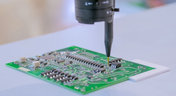
Unlike the clumsy human finger, a thermal camera can detect minute temperature differences across its view. This allows you to rapidly identify any components that are consuming current. Any parts or areas of your board that draw current will also generate heat that can easily be picked up by a thermal camera.
Blog
•
Complete Guide to DIY SMT Assembly In Your Office
I want to share a little secret with you in this article: Assembling SMT prototypes boards is not only easy, but it requires very little equipment. Using just a stencil, I can easily hand prototype down to 0.3 mm pitch ICs, and 0201 (imperial) sized passive components. If you’re currently hand assembling boards with a soldering station, you need to stop this immediately and start using a stencil instead!

Blog
•
State of the Electronics Industry 2021
With the challenges of 2020 behind us, what challenges and opportunities lie ahead for hardware designers in 2021? In this article Vince Mazur, Technical Product Marketing Engineer at Altium, looks ahead to three emerging trends and share steps to address each one successfully in the year ahead.

Blog
•
The Mysterious 50 Ohm Impedance: Where It Came From and Why We Use It
When we talk about S-parameters, impedance matching, transmission lines, and other fundamental concepts in RF/high-speed PCB design, the concept of 50 Ohm impedance comes up over and over. Look through signaling standards, component datasheets, application notes, and design guidelines on the internet; this is one impedance value that comes up repeatedly. So where did the 50 Ohm impedance standard come from and why is it important?

Blog
•
Keeping Your Circuits Dry
For the home hobbyist, protecting their electrical devices usually means keeping the coffee cup or soda can away from anything that carries a large voltage. Good practice indicates that electrical devices should be housed in an enclosure to protect expensive components and reduce the risk of electric shocks from exposed circuitry. However, what do you do if the fantastic new device you’ve designed needs to work in a humid, damp, or dripping wet environment?
Blog
•
Tips for Updating Old PCB Designs with New Parts
Have you ever opened up an old design and wondered how much of it was still usable? Maybe you were contacted by an old client, and they want you to provide some updates on an old design. No matter what the situation is, there are times where updating old PCB designs with new parts makes sense. If done correctly and when armed with all the right information up front, you can cut down the total design time while preserving the best parts of your design in a new iteration. Here’s what you can do to update your old designs successfully and how your PCB design features can help.

Blog
•
How to Involve Customers in PCB Product Development
The more complex the product gets, the more involved your customer will need to be to ensure you’re designing to their requirements. When you’re using a data sharing system that integrates with your PCB design tools, it’s easy to give your customers visibility into the product development process. Altium 365 is the only system that integrates with Altium Designer® and gives you the ability to give anyone access to your PCB projects, including your customers and manufacturer.


Your search returns no results.


