News & Updates

NEW

Blog
•
Why Modern Electronics Teams Are Moving to a Cloud ECAD Platform
Great products are built by connected teams, not disconnected tools. This article shows how cloud ECAD platforms enable real-time co-design, structured design reviews, and seamless collaboration across engineering, manufacturing, and supply chain teams.

NEW

Blog
•
10 Questions to Ask Your Fabricator Before Submitting a Rigid-Flex Design
A five-minute conversation with your fabricator could save weeks of redesign. Discover the ten questions that can improve manufacturability, boost yield, and help your rigid-flex project succeed on the first build.

Blog
•
Who Needs Integrated Electronic Component Search
Finding the right component shouldn't mean searching through dozens of websites and datasheets. This article shows how integrated component search helps engineers select parts faster while reducing sourcing risks and design delays.


Blog
•
How BOM Portal Supports R&D and Procurement with DFM & DFC Analysis Throughout the Entire Product Lifecycle
The best sourcing decisions happen when procurement is involved early. This webinar demonstrates how BOM Portal gives both engineering and procurement access to live lifecycle, pricing, compliance, and availability data to drive smarter decisions from prototype through production.

Blog
•
How to Design a PCB: From Schematic Capture to Manufacturing
This article walks through the complete PCB design workflow, from schematic capture and component selection to layout, design reviews, and manufacturing documentation. It highlights the key decisions at each stage that help engineering teams produce reliable, manufacturable products.


Blog
•
5 Power Integrity Myths: AC Edition
The biggest threat to your power integrity might be outdated design advice. This article challenges five common AC power integrity myths and shows what really matters when designing today's high-speed PCBs.


Blog
•
Your Design Data Has Zero Defense
Your design data may be more exposed than you think. This webinar shows how to identify common security gaps and secure engineering workflows with centralized access control and governance.


Blog
•
Flex Circuit Coverlay: Design with Lamination Processes In Mind
Your flex PCB may look perfect in CAD but coverlay doesn't stay perfectly still during manufacturing. This article reveals why designing for lamination behavior is one of the most important steps in building reliable flex circuits.


Blog
•
Integrated PCB Design vs. Legacy Point Tools: What’s the Real Cost?
As hardware development grows more collaborative, disconnected point tools can introduce data inconsistencies, traceability gaps, and costly coordination challenges. This article examines how integrated PCB design environments connect design, mechanical, supply chain, and review workflows to improve efficiency throughout the product lifecycle.

Blog
•
Make Better Design Decisions with Signal and Power Integrity Insight
Signal integrity and power integrity are closely connected, with problems in one often affecting the other as designs become faster and more complex. This webinar explains how integrated analysis workflows help engineers evaluate PDN performance, identify potential issues early, and improve overall design quality.

Blog
•
Optimizing Your Electronics Product Design Workflow and Eliminating Bottlenecks
Every manual handoff adds time and risk to the product development process. This article shows how modern design workflows automate routine tasks, improve data visibility, and help engineering teams focus on innovation instead of administration.

Blog
•
Top Tips from Experienced Flex Designers
This article describes the best hints and tips for designers of rigid-flex circuits. These tips include choosing the most appropriate material, suggestions for coordinating the PCB with the manufacturer, and a set of rules to be followed while PCB design.

Blog
•
How Do Capacitor Mounting Structures And Footprints Impact Total Inductance?
There are a number of factors at play when it comes to the impact of inductance on high-frequency power distribution systems. This article will focus on the inductance of the capacitor footprint along with the inductance of vias from the capacitor footprint to the PCB power planes. Included are the various types and sizes of footprints for ceramic capacitors as well as a footprint for a tantalum capacitor; how changing the footprint impacts inductance and test results obtained for different capacitors.
Blog
•
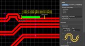
How to Perform Differential Pair Tuning in Altium Designer 20
In order to properly suppress common-mode noise, differential pairs must be routed in parallel, with perfect symmetry, and with matched lengths. In real PCBs, meeting these three objectives isn’t always possible. Instead of eyeing out your different pair lengths, the interactive routing tools in Altium Designer make differential pair length matching easy. You can encode permissible length mismatches as design rules as part of controlled impedance routing, or you can manually perform differential pair tuning using a variety of meandering styles. Here’s how this works in Altium Designer.

Blog
•
Driving Haptic Vibration and Feedback in Wearables
Augmented reality, virtual surgery, limb replacements, medical devices, and other new technologies need to incorporate haptic vibration motors and feedback to give the wearer a full sense of how they are interacting with their environment. Unless these cutting-edge applications include haptic vibration and feedback, users are forced to rely on their other four senses to understand the real or virtual environment.

Blog
•
Back Drilling Example in Altium Designer: One of the Easiest Ways to Improve Signal Integrity
Over the last 20 years, electronic devices have become increasingly sophisticated. Less than two decades ago, just having a mobile phone to make calls was rare; today, our phones power our lives. To meet the growing demand for smartphone technology, technology has become faster, more functional, and intuitive. Improvements to the component base have streamlined processes while reducing manufacturing costs.

Blog
•
Is it Simultaneous Switching Noise or Crosstalk?
Going deeper into crosstalk, there is always the issue of verifying EMI/EMC compliance through test and measurement. With the multitude of signal integrity problems that can arise in real PCBs, how can the astute designer distinguish them all? Some problems are clearer than others, with specific signal integrity measurements being developed for testing and measuring particular aspects of signal behavior. The fact is, multiple signal integrity problems could be present on a single interconnect simultaneously.

Blog
•
Sharing PCB Data with Manufacturers in the Cloud
Once you’ve finished your new project and you’re ready to push it to your manufacturer, you’ll normally be stuck in an endless email chain with an engineer, or you’ll have to share cloud links with each other. The cloud sharing and design release tools in Altium Designer and Altium Concord Pro are a huge help in this area. In this post, I’m going to take an existing project I’ve worked with in a number of recent blogs, create some fabrication and assembly documentation, and finally push this data to a manufacturer using Altium Concord Pro.

Blog
•
The Great PCB Layout "Rules of Thumb" Debate Rages On
To this day, I still see many PCB layout “rules of thumb” that first became common nearly 20 years ago. Do these rules still universally apply? The answer is a firm “maybe.” The discussion around PCB layout rules of thumb is not that these rules are correct or incorrect. The problem is that the discussion around these rules often lacks context, leading to the always/never type of discussion seen in some popular forums. My goal in this article is to communicate the context behind the common PCB design rules.

Blog
•
How to Design Your PCB Test Coupon and What You Can Test
As the operating speed of components has increased, controlled impedance is becoming more common in digital, analog, and mixed-signal systems. If the controlled impedance value for an interconnect is incorrect, it can be very difficult to identify this problem during an in-circuit test. However, testing is normally performed on a PCB test coupon, which is manufactured on the same panel as the PCB. If you want to get through board spins quickly and aid future designs, you might consider designing a test coupon and keeping it handy for future designs.

Blog
•
Altium DbLibs and Electronic Components in the Cloud with Altium Designer 20.1
Altium’s DbLib support is one of the oldest and most loved features of Altium Designer for managing electronic components and their data. They’ve been present in the software world since before I could fathom the existence of Ohm’s law. Altium 20.1’s new Component Sync feature allows you to synchronize virtually any database or database Library with Altium 365, taking advantage of both approaches strengths.
Blog
•
What is a Schematic Netlist for Your PCB?
If you’ve created your next great schematic, there is a lot going on behind the scenes in your design software. A schematic netlist is one of the central pieces of information that will be used in multiple features in your design software to create a real PCB. Your schematic netlist provides both electrical connectivity information, and reflects the functional structure of your design data in a single set of data.
Blog
•
How to Select an Inductor for a Buck Converter
An SMPS is one of those quiet (yet electrically noisy) devices that makes your favorite electronics run smoothly. Among the numerous DC-DC converter topologies, a buck converter finds plenty of uses for stepping down the input voltage to a lower level while providing high efficiency power conversion. A common question around component selection for these power converters is how to select an inductor for a buck converter. The goal in working with an inductor and other components in a buck converter is to limit power loss to heat and while minimizing current ripple.

Blog
•
US Department of Transportation Seeking Alternatives to GPS
GPS-capable devices range from your phone to your smartwatch; simply type in your destination and follow the directions. Simple, right? According to the Washington Post, we should all stop using GPS as it’s ruining the navigation centers of our brains. Despite the neurological effects on perception and judgment, the U.S. Department of Transportation (DOT) aims to find alternatives to GPS to provide redundancy.

Blog
•
Bluetooth 5.1 SoC vs. Module: Which is Best for Your Design?
The list of features available in Bluetooth just got a little longer since the release of Bluetooth 5.1. If you want to incorporate a Bluetooth 5.1 SoC into your new product, you have two primary options for bringing this component into your board. The first is as an SoC that mounts to your board just like any other component. The other option is to bring a module into your new board—directly onto the surface layer. Here’s what you need to know about a Bluetooth 5.1 SoC or module in your next IoT product.

Blog
•
Altium 365 Getting Started User Guide - Available Now
Get Started with Altium 365 with a step-by-step guide and videos to experience the most connected experience for PCB design and realization: https://my.altium.com/altium-365/getting-started/

Blog
•
USB Power Delivery for Your Next Project
Since its introduction in the late 90s, the USB standard has never ceased to grow in popularity. There has been a growing trend toward USB being a power delivery interface with data, rather than a data interface that can supply power, as the 1.0 specification originally intended. To supply the increasing thirst for power over USB, the USB 3.0 Spec with Type-C began implementing the Power Delivery standard, which you should consider using for your next electronics project.



On-Demand Webinar
•
Jun 12, 2025
Proactive Lifecycle Management: Preventing Obsolescence Before It Hits


On-Demand Webinar
•
Apr 23, 2025
Collaborative Design Review: Ensuring Quality from Schematics to Supply Chain

On-Demand Webinar
•
Apr 22, 2025
From Prototype to Production: Optimizing BOM Costs Without Compromising Quality with Part Analytics



On-Demand Webinar
•
Apr 9, 2025
Component Selection in Altium Designer: Making Data-Driven Decisions with Data Integrations

On-Demand Webinar
•
Mar 25, 2025
Unlocking the full potential of your design team with Altium's enterprise solution


On-Demand Webinar
•
Jan 24, 2024
Discover How Altium Designer 24 Revolutionizes Team Dynamics in PCB Design


