News & Updates

NEW

Blog
•
How to Solve Fit, Form, and Function Challenges in Robotics with ECAD-MCAD Collaboration
As robotics systems become increasingly miniaturized and intricate, ensuring perfect fit, form, and function across electrical and mechanical domains is critical to avoid design setbacks. Real-time ECAD-MCAD integration with two-way sync empowers teams to streamline workflows, reduce PCB rework, and deliver more reliable designs faster.

NEW

Blog
•
One Vision, Three Powerful Solutions: Introducing Altium Discover, Altium Develop, and Altium Agile
We are excited to announce the launch of three new platform-based solutions that will transform the way electronic products are designed, built, and delivered: Altium Discover, Altium Develop, and Altium Agile. These solutions are designed to simplify processes, accelerate innovation, and make collaboration seamless across the entire electronics lifecycle. Together, they realize the purpose of Altium and Renesas: To Make Our Lives Easier.

Blog
•
The Cost of Overreaction: How Misguided Orders Disrupt the Semiconductor Market
Discover how short-sighted ordering practices fuel volatility in the semiconductor market and why smarter, data-driven approaches are key to building resilience and sustainability.


Blog
•
The Top 5 Workflow Bottlenecks Slowing Down Mechanical Engineering Teams
Mechanical engineering teams frequently encounter delays from fragmented communication, disconnected toolchains, and inefficient synchronization processes. This article examines five critical workflow bottlenecks and highlights how ECAD-MCAD integration with real-time, bidirectional updates can eliminate rework and accelerate design iterations.


Blog
•
Optimize Your Multiboard PCB System with Intelligent Design and Manufacturing Solutions
Optimizing multiboard PCB systems demands visibility across logical, physical, and manufacturing domains. This article outlines how Altium’s environment lets engineers establish system‑level schematics, 3D spatial validation, harness documentation, and synchronized outputs to streamline design and production.

Blog
•
Why Mechanical Engineers Struggle With ECAD Collaboration (And How to Fix It)
If you’ve ever been frustrated by clunky PCB-to-mechanical workflows, you’re not alone. Learn why collaboration between mechanical and electrical engineers is harder than it should be and what’s behind the struggle.


Blog
•
Digital Thread for Electronics: Synchronizing PCB, Multi-Board, and Harness Design
Eliminate costly mismatches and assembly delays. This whitepaper shows you how to apply a unified digital thread across PCB, multi-board, and harness workflows - bridging ECAD/MCAD silos, ensuring connector accuracy, mechanical fit, and real-time collaboration for flawless system design.


Blog
•
Building a Model Context Protocol Server for Arduinos
This guide walks you through creating an MCP server that turns AI interactions with Arduino into a predictable, automated process handling tasks like board listing, compilation, and serial communication via a fast, menu‑driven interface. Skip the guesswork of prompt nudging and reduce the risk of unintended device issues.


Blog
•
Zero Voltage Switching in DC/DC Converters
Our brand-new article explains how zero-voltage switching improves performance in DC/DC converters through reduced losses, lower EMI, and smarter gate-drive control.


Blog
•
Getting Started with the GreenPAK Introduction Kit
Take your first steps into mixed-signal design with the Renesas GreenPAK Introduction Kit. Ari Mahpour shows how to design, simulate, and validate a clock divider project, making it easy for beginners to start experimenting with programmable mixed-signal devices.


Blog
•
Smarter Electronic Part Sourcing for Automotive Purchasing Professionals
Targeted at procurement professionals in the automotive industry, the article outlines the evolving pressures of sourcing components for electrified and connected vehicles. It highlights Octopart’s ecosystem as a unified tool that centralizes availability, compliance, pricing, and lifecycle intelligence to optimize sourcing efficiency.

Blog
•
Improving Supply Chain Success with BOM Management
It’s no secret that component shortages have become more frequent this year. Companies will continue to grapple with supply chain challenges into 2022 and beyond. The impact of manufacturing delays can be substantial if a part is not available. Delays occur and sales plans get put on hold. It can also be very expensive and risky to replace parts from multiple sources. Fortunately, many shortages can be avoided by introducing proactive supply chain practices.

Blog
•
Overview of PCB/PCBA Reliability and Failure Analysis
Reliability testing and failure analysis of a PCB/PCBA go hand-in-hand; when designs are stressed to the limit, their failure modes need to be determined through thorough inspection and analysis. To get started on this topic, it’s important to understand the qualification aspects that will govern your bare board design and the PCBA. We’ll look at the various dimensions of PCB/PCBA reliability, as well as some of the standard failure analysis techniques used to identify potential design change requirements.

Blog
•
When Do PCB Power Plane Resonances Occur?
By now, designers should be aware of some important behavior involved in power delivery to components in a PCB, particularly for digital components. All digital components produce and manipulate wideband signals, where the frequency content theoretically extends up to infinite frequency. As such, some radiation may propagate through your PCB, leading to resonant behavior that is not observed on the power rail.

Blog
•
How to Choose PCB Plating for Your Finished Board
Once your board passes through the standard PCB fabrication process, the bare copper in your PCB will be ready for the application of a surface finish. PCB plating is applied to protect any copper in your PCB that would be exposed through the solder mask, whether it’s a pad, via, or other conductive element. In this article, I’ll run over the different PCB plating material options and their advantages in your PCB.

Blog
•
What is the PCB Supply Chain?
The PCB supply chain encompasses multiple components, raw materials, and the PCB itself. PCBs and PCB assemblies are often the most technically complex components that are purchased for electronic assemblies and products. The complexity of modern PCBs leads to several challenges for a supply chain management team that may be significantly different when compared with other commodities the team manages. In this brief guide, we'll look in-depth at the PCB supply chain, and specifically what falls within the purview of a procurement and supply chain management team.

Blog
•
A Guide to Mode Conversion, Its Causes, and Solutions
On interconnects, such as board-to-board connections or cascaded transmission line arrangements, you have an important EMC compliance metric that is sometimes overlooked. This is mode conversion, which can be visualized in an S-parameter measurement for differential and common-mode signal transmission. In this article, we’ll look at a short overview of mode conversion in high-speed design with some examples from common differential standards.

Blog
•
PCB Via Size and Pad Size Guidelines
There are some aspects of PCB design and layout that seem deceptively simple, and yet they have a complex answer that is related to many important aspects of manufacturing. One of these design aspects is the match between PCB via size and pad size. Obviously, these two points are related; all vias have a landing pad that supports the via and provides a place to route traces into a via pad. However, there are some important sizing guidelines to follow when the matching pad and via sizes, and this match is an important element of DFM and reliability.

Blog
•
Differential Microstrip Impedance Calculator
Are you looking for a free tool that you can use to calculate the impedance of differential microstrips? We created a simple tool you can use to calculate differential microstrip impedance for a given geometry and dielectric constant. If you’ve been looking for an accurate differential microstrip impedance calculator, then the calculator below is certainly one of the best free tools you’ll find on the internet before you start using field solvers to determine differential pair impedance.

Blog
•
Getting Through a PCB DFM Check
In this article, we’ll discuss the key design features to implement, and steps to take prior to fabrication that will help prevent some common DFM problems. I’ll also provide examples of where I commonly see these PCB DFM problems in signal integrity circuits.

Blog
•
What is Spreading Inductance?
If you’re working with a high-speed digital component, there are some simple power integrity rules that should be followed. However, there is one quantity that is sometimes ignored when building a PDN impedance simulation: the spreading inductance of your plane pair. Here are some points designers should know about the spreading inductance of a plane pair.

Blog
•
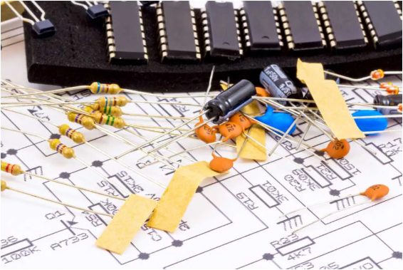
PCB Design Basics for New Designers
In this article, I’ll present some design basics that every new designer should follow to help ensure their design process is successful. Some of these points may challenge the conventional view of how circuit boards are constructed, but they are intended to help balance low noise signaling, manufacturability, and ease of solving a layout.

Blog
•
Selecting Materials for High Voltage PCB Design and Layout
High voltage PCBs are subject to certain safety and reliability concerns that you won’t find in most other boards. If your fabrication house specializes in high voltage PCBs and keeps materials in stock, they can likely recommend a material set, as well as a standard stackup you might use for certain voltage ranges and frequencies. If you need to choose your own materials, follow the tips below to help you narrow down to the right material set.

Blog
•
When to Use Tented Vias in Your PCB Layout
There are some guidelines I see many designers implement as a standard practice, often without thinking about it. Some of these practices are misunderstood or implemented without best practices. Others are implemented without thinking about the potential problems. One of these is the use of tented vias, which is sometimes implemented in a PCB layout by default. Is this always the right practice?

Blog
•
How to Impedance Match and Terminate Capacitive Loads
The idea of a purely capacitive load is something of a fallacy. Yes, capacitors exist, but all capacitors are non-ideal, and it is this deviation from a theoretical capacitance that determines how to impedance match a load that exhibits capacitive behavior. Let’s take a look at this important aspect of interconnect design and see what it really means to terminate a capacitive load.

Blog
•
Using Altium 365 Over Your Vanilla Version Control System
There are all sorts of version control systems out there that people have been using with their PCB design software. As discussed in Why Use a Version Control System, we looked at different options ranging for local hard drive storage to sophisticated online revisioning systems. In this article we will be reviewing the differences between a standard VCS and Altium 365.

Blog
•
Why Use a Version Control System in PCB Design
Version Control Systems (VCS) have been around for many decades within the software world but can be surprisingly new to some folks in the electronics design industry. This article will cover what a VCS is, what it does, and why you should be using one for your PCB design projects.


On-Demand Webinar
•
Jun 12, 2025
Proactive Lifecycle Management: Preventing Obsolescence Before It Hits


On-Demand Webinar
•
Apr 23, 2025
Collaborative Design Review: Ensuring Quality from Schematics to Supply Chain

On-Demand Webinar
•
Apr 22, 2025
From Prototype to Production: Optimizing BOM Costs Without Compromising Quality with Part Analytics


On-Demand Webinar
•
Apr 9, 2025
Component Selection in Altium Designer: Making Data-Driven Decisions with Data Integrations

On-Demand Webinar
•
Mar 25, 2025
Unlocking the full potential of your design team with Altium's enterprise solution


On-Demand Webinar
•
Jan 24, 2024
Discover How Altium Designer 24 Revolutionizes Team Dynamics in PCB Design