News & Updates

Blog
•
PCB Design Process: The EDA Design Approach
Dive into how a modern EDA workflow transforms PCB design by linking electrical, mechanical, and manufacturing requirements from idea to final release. With constraint‑driven integration, you can cut down on respins and bring better boards to market faster.
Blog
•
Getting Started for Mechanical Engineers
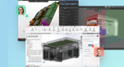
Explore our collection of MCAD Collaboration walkthroughs, where you’ll discover how to synchronize mechanical constraints and keepouts, maintain traceability with advanced history and revision control, and streamline electromechanical connectivity through harness synchronization. These topics and many more are covered in this article.


Blog
•
Are Your ECAD Tools Holding Back Engineers’ Productivity?
The article highlights that productivity issues often stem from tool limitations rather than engineer effort, especially as project complexity grows. ECAD tools that offer clear version control, cross-discipline integration, and workflow awareness are key to sustaining efficiency.

Blog
•
How Integrated PCB Design Cuts Development Time for Complex Electronics
Fewer tool handoffs, fewer errors, and smoother collaboration that’s the power of integrated PCB design. Learn how unifying your design environment can cut development time and help you deliver complex electronics faster.
Blog
•
Registration Challenges in UHDI: Why Fabrication Tolerances Matter in Your Layout
As UHDI structures shrink, achieving accurate layer-to-layer registration becomes less forgiving than ever. Learn why fabrication tolerances matter so much in ultra-fine geometries and how to design with registration limits in mind from the start.


Blog
•
How Engineering Project Management Tools Are Changing Engineering Teams’ Productivity
Engineering project management tools play a critical role in managing timelines, resources, and cross-disciplinary coordination. This article breaks down the most impactful systems for improving execution and team performance.


Blog
•
7 Ways to Catch Rules & Constraints Early – Checklist
Discover seven actionable ways to spot and fix rules and constraint issues before they derail your PCB project. Using Altium Designer Agile, these tips help you build more manufacturable and reliable boards with fewer iterations.
Blog
•
Do You Need an IPC-D-356 Netlist?
If your output package is Gerber-based, adding an IPC-D-356 netlist can dramatically improve how your design is reviewed and validated for production. Here’s when it matters, what it contains, and how to generate it quickly in Altium.

Blog
•
How Agile BOM Management Helps You Lock in Pricing Before Market Shifts
When engineering and procurement work from different BOM versions, delays and cost surprises follow. Learn how agile BOM management brings teams onto one connected BOM so they can respond fast, manage risk, and lock pricing early.

Blog
•
Flexible Circuits: Enhancing Performance with Shielding, Heat Dissipation, and Stiffeners
A flex circuit can look perfect on paper and still fail in the real world due to EMI, hot spots, or mechanical strain. This article breaks down how shielding, thermal planning, and stiffeners help deliver designs that stay reliable over time.

Blog
•
PCB CoDesign: Design Faster Together
Experience accelerated design collaboration with PCB CoDesign, exclusively available on Altium Designer starting from December 13th. This innovative feature adopts a collaborative approach by seamlessly integrating schematic and PCB design, enabling multiple engineers to work on the same project. Explore this cutting-edge feature on our newly launched page dedicated to its functionalities.

Blog
•
6 Steps to Accelerate the Development of Complex Products
Learn the key lessons from the presentation at Iteration22; “Joe Justice, Wikispeed - Everyone Must Be a Chief Engineer at SpaceX.” Read on and discover how to speed up the development of complex products.
Blog
•
Design Phase – Lid Assembly Mechanics Part 2
We are continuing our journey into lid assembly mechanics inside the Open Source Laptop Project. In this chapter, we are focusing on the sensor PCB above the display panel.

Blog
•
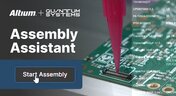
How to Speed Up Your Manual Assembly Process with Assembly Assistant? The Story of XVP Photonics
Are you struggling with your manual assembly process? Would you like to speed it up and improve component placement accuracy? Read the story of XVP Photonics; with Assembly Assistant, they improved the component placement time by 25%. Discover how!

Blog
•
45V-5A Adjustable Half-Bridge DC to DC Converter
DC-to-DC buck converters are extensively employed in electronic devices. In this article, we will introduce you to one of our new projects—a DC-to-DC converter designed to serve as a power supply as well.
Blog
•
The Challenges of Modern Design: Why Requirements Management Is Essential
You need a robust requirements management process to ensure your design intent communication stays clear and organized. Read on to explore the crucial connection between well-managed requirements and today’s design.

Blog
•
Efficiency And Noise Top 10 Switching Regulator Modules
Switching regulator modules have become indispensable in a wide array of electronic devices, providing a more efficient means of voltage conversion between different levels by storing and releasing energy. Explore further insights into these devices in today's dynamic world of electronics.
Blog
•
Add USB Type-C Power Delivery to Your Designs!
We want to invite you to explore the fundamentals of USB Type-C Power Delivery which is now the most popular energy transmission in current times. We will show you how to easily incorporate a dedicated PD IC into your own designs.
Blog
•
Design Phase – Lid Assembly Mechanics Part 1
It is time to delve deep into the mechanical design of our Open Source Laptop project. In this article we give you an update about the first part of fitting elements into the system. You will learn more about laptop lid, webcam integration, light sensor and microphones which will be used in this project.

Blog
•
How to Design for Test in Embedded Systems
Whether you're designing a high-speed PCB, or a complex embedded system, it will need some level of testing. In this article, we will show you some simple tricks that can make testing and debugging a prototype much easier.
Blog
•
Crosstalk Basics in PCB Design
Crosstalk is one of the most common issues related to electronics. Learn the basics of this phenomenon in PCB design, and gain knowledge on how to avoid it in your projects.
Blog
•
Top 3 Multi-Board PCB Connectivity Errors
Preparing complex PCB designs can often keep you awake at night. Learn more about some of the most common issues encountered in multi-board electrical connections.

Blog
•
Access to your Training Certificates on My Altium
Introduce an update on the My Altium user page that highlights your certificates and tracks your training progress, with one-click access to the Training Dashboard and Training Catalog pages. Easily view and share your certificates, keep an eye on your learning journey, and explore a variety of training resources.

Blog
•
Rigid-Flex PCBs: Advantages and Challenges
In this article, we will begin with a basic explanation of how rigid-flex technology differs from rigid board technology. We will then provide an overview of the advantages and conclude with a discussion of the challenges to be aware of.
Blog
•
When Should You Use Intrusive Soldering?
Through-hole components are frequently employed in power electronics, particularly when dealing with AC power from a wall outlet. In this article, you can delve into the intrusive soldering process and discover when it can be applied in PCB design.
Blog
•
Unveiling the Crucial Role of PCB Harness Design Capabilities in Multi-Board Designs
Multi-board designs are the key to meeting evolving demands, requiring robust PCB Harness Design for seamless interconnection and success. Join us as we explore the importance of PCB Harness Design capabilities and how they are crucial for the success of multi-board designs.


Your search returns no results.


