News & Updates
Blog
•
Beyond Traces: Why Soldermask May Be the Critical Factor in Ultra HDI
In ultra-HDI designs, soldermask is no longer a passive coating but a pivotal element that can determine manufacturability. This article explores why mask registration, resolution, and feature tolerances become critical as line spacings shrink below 50 µm.

Blog
•
How ECAD-MCAD Co-Design Supports Aerospace Reliability and Compliance
When the margin for error is nearly zero, aerospace engineering demands a design process that’s seamless across all domains. Here, we explore how ECAD-MCAD co-design delivers an integrated workflow that supports first-pass success and compliance with strict aerospace standards.


Blog
•
Most Common Causes of PCB Assembly Rework and Scrap
Many PCB assemblies fail not because of exotic faults, but due to basic issues like incorrect BOM entries or footprint mismatches that force rework or scrap. This article dives into the most common causes and how to prevent costly defects in your design-to-manufacturing process.


Blog
•
Behind the Scenes with AI Embedded Development
Forget one-shot AI hacks Ari Mahpour shows the thoughtful, sustainable way to integrate AI into embedded firmware development. Learn the core principles (planning gate, HAL abstraction, observability, timeout design) that can help you push your efficiency 5-10 times in real hardware projects.


Blog
•
We're heading to PCB West 2025!
Join Altium at PCB West 2025 in Santa Clara, CA, on October 1! Stop by Booth 300 for the official launch of the new Altium platform, built on the foundation of Altium Designer and Altium 365. Be sure to check out our live demos of Altium Develop and Altium Agile.

Blog
•
Peak Electrical Performance in Multi-Board Designs With Advanced Simulation and Compliance Tools
Moving from single-board to multi-board systems is a leap in complexity. You must manage not just routing, but power, signal integrity, mechanical fit, and regulatory requirements across boards. In this article, you’ll discover how Altium’s advanced simulation and compliance tools help engineering teams overcome these challenges and deliver reliable multi-board solutions.

Blog
•
How to Catch Enclosure and Connector Misalignment Before the First Prototype
As electronics continue to miniaturize and functionality increases, even minor misalignments between enclosures and connectors can derail a project. This article explores how early integration of ECAD and MCAD workflows helps detect and eliminate those costly issues before the first prototype is built.


Blog
•
Executive Insights Into Electronic Product Development Gaps You Need To Close
Electronics hardware development is falling behind broader product development disciplines due to fragmented workflows, poor collaboration, and limited compliance visibility. This gap introduces risk, delays, and missed opportunities but executives see real business value in modernizing electronics development through better integration, traceability, and lifecycle visibility.


Blog
•
Sourcing For High-Mix Low-Volume Electronics Manufacturing
High-mix, low-volume (HMLV) electronics manufacturing requires agile sourcing strategies to handle shifting BOMs, erratic lead times, and component volatility. All while controlling costs and ensuring compliance. Cloud-based tools like Altium provide real-time component visibility, BOM collaboration, and supplier integrations to help navigate HMLV complexities.


Blog
•
How to Solve Fit, Form, and Function Challenges in Robotics with ECAD-MCAD Collaboration
As robotics systems become increasingly miniaturized and intricate, ensuring perfect fit, form, and function across electrical and mechanical domains is critical to avoid design setbacks. Real-time ECAD-MCAD integration with two-way sync empowers teams to streamline workflows, reduce PCB rework, and deliver more reliable designs faster.

Blog
•
One Vision, Three Powerful Solutions: Introducing Octopart Discover, Altium Develop, and Altium Agile
We are excited to announce the launch of three new platform-based solutions that will transform the way electronic products are designed, built, and delivered: Octopart Discover, Altium Develop, and Altium Agile. These solutions are designed to simplify processes, accelerate innovation, and make collaboration seamless across the entire electronics lifecycle. Together, they realize the purpose of Altium and Renesas: To Make Our Lives Easier.

Blog
•
Part Selection Fundamentals: Creating Resilient Component Requirements
Learn how to ensure electronic components meet the demands of harsh environments. This article explores key standards, testing protocols, and design considerations for building resilient systems that perform reliably under extreme conditions.
Blog
•
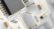
Printed Electronics: The Future of Flexible and Cost-Effective Circuit Design
This article explores the rise of printed electronics as a lightweight, flexible, and cost-effective alternative to traditional PCB design. It highlights key benefits like reduced manufacturing costs, sustainability, and new design possibilities—especially in wearables, medical devices, and automotive applications.

Blog
•
How to Choose the Best Requirements Management Tool for Electronics Development
Many electronics teams still rely on documents and spreadsheets for requirements management—leading to gaps, errors, and delays. Alexsander Tamari explores better tools to improve traceability, collaboration, and project outcomes.
Blog
•
New Routing Possibilities with Ultra HDI
Explore how Ultra HDI technology is redefining PCB design. This article breaks down the benefits and manufacturing considerations of Ultra HDI, and how it enables next-level routing density and miniaturization in advanced electronics.
Blog
•
3D-MID in Focus: Principles, Processes, and Practical Use
This article introduces 3D-MID (Mechatronic Integrated Devices), a technology that integrates circuitry into 3D plastic structures to reduce size, weight, and complexity. It explains the production process, use cases, and benefits of 3D-MID in sectors like automotive, medical, and consumer electronics.
Blog
•
Eliminate EMI and Signal Integrity Issues in Multi-Board PCB Designs
Ensure signal integrity and minimize EMI in complex electronics. Our new article explains how to address electromagnetic interference and signal integrity challenges in multi-board PCB designs, offering practical strategies and layout considerations for reliable system performance.

Blog
•
How to Overcome Power Distribution and Connector Misalignment Challenges in Multi-Board PCB Systems
Connector misalignment can compromise the reliability of power delivery in multi-board systems. This article explores the causes, effects, and prevention strategies for connector misalignment in power distribution, helping you design more robust multi-board PCB systems.

Blog
•
Mastering Component Templates in Altium Designer 25
Our new article by Dario Fresu explains how Component Templates in Altium Designer 25 Pro improve design consistency, reduce errors, and streamline collaboration. It highlights practical benefits like standardized naming, faster component creation, and scalability across projects. Includes examples of using templates with Altium 365™ to simplify complex component setup.
Blog
•
Wire Harness Design Guide for Development and Manufacturing
Designing a wire harness goes far beyond just connecting components—it’s about ensuring manufacturability, reliability, and compliance. This article walks you through the entire process, from initial design to production, helping you streamline development and avoid common pitfalls.

Blog
•
Preparing for Medical Device Cybersecurity Assessments
Explore the key considerations and best practices for conducting cybersecurity assessments in medical device development. This article outlines how to identify potential threats, evaluate risks, and ensure compliance with evolving industry standards.
Blog
•
Harness Complexity, Design with Simplicity
Harness Design in Altium Designer simplifies managing PCB interconnections, ensuring reliable performance and streamlined manufacturing. With logical connectivity tools, harness layout drawing, and manufacturing-ready documentation, it keeps your designs efficient and organized—all within a unified design environment. Perfect for automotive, aerospace, and industrial applications.

Blog
•
Getting Started with NVMe and the Raspberry Pi 5
Our new article guides you through enhancing your Raspberry Pi 5's performance by setting up NVMe SSD storage using an expansion HAT. It covers the benefits over traditional MicroSD cards, including improved speed and reliability, and provides step-by-step instructions for installation and configuration.

Blog
•
Why Human Error Is Electronics Design Cybersecurity's Biggest Weakness
Human error is a leading cause of cybersecurity breaches—even in electrical engineering. Our article explores how everyday design and collaboration habits can create vulnerabilities, and what engineers can do to build safer, more secure workflows.
Blog
•
From Concept to Production: A Modern Approach to Wire Harness Engineering
Discover how modern wire harness engineering is evolving to meet the growing complexity of electrified systems. This whitepaper explores best practices, intelligent automation, and ECAD-MCAD collaboration to improve efficiency and reduce errors. Download now to stay ahead in an increasingly connected world.
Blog
•
Transforming RF Design with Ultra HDI
Ultra-HDI technology is transforming RF design by enabling finer line widths, improved signal integrity, and more compact, high-performance boards. Our brand-new article explores its advantages over traditional methods and the benefits of integrating flexible circuits.

Blog
•
Boost Your PCB Testing Efficiency with Testpoint Manager
Testpoints are essential for efficient PCBA testing and debugging. Our latest whitepaper dives into testpoint optimization, fault detection, and automated testing strategies, along with a full tutorial on using Testpoint Manager in Altium Designer. Discover how to streamline your testpoint assignments and improve measurement accuracy!
















Your search returns no results.


