News & Updates

Blog
•
Altium Designer 22.6 Update
We are happy to announce that the Altium Designer 22.6 update is now available. Altium Designer 22.6 continues to focus on improving the user experience, as well as performance and stability of the software, based on feedback from our users. Check out the key new features in the What's New section on the left side of this window!

Blog
•
Join PCB Design Review Competition from Altium
Find 9 mistakes in a PCB design and get added into the lucky draw to win a prize from Altium!


Blog
•
SAP (Semi-Additive PCB Process) – Top 5 Questions Regarding Stack Up
This Semi-Additive Process is an additional tool in the PCB fabricators' toolbox that enables them to provide feature sizes for trace width and spacing that are 25 microns, (1 mil) and below depending on the fabricators' imaging equipment. This provides much more flexibility to breakout out tight BGA areas and the ability to shrink overall circuit size and/ or reduce the number of circuit layers in the design. As the PCB design community embraces the benefits of this new printed circuit board fabrication technique, there are of course many questions to be answered.



Blog
•
Improving Supply Chain Success with BOM Management
It’s no secret that component shortages have become more frequent this year. In fact, countries around the world are losing billions in revenue due to supply issues. Having the right components on hand is more crucial than ever as availability, obsolescence, counterfeit products and environmental non-compliance risks continue to grow. Fortunately, many shortages can be avoided by introducing proactive supply chain practices.
Blog
•
What is the Impedance of Length-Tuning Structures?
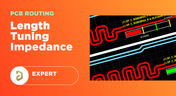
Do length-tuning structures create an impedance discontinuity? The answer is an unequivocal “yes”, but it might not matter in your design depending on several factors. Applying a length-tuning structure is equivalent to changing the distance between the traces while meandering. Therefore, you will have a change in the odd-mode impedance of a single trace. The question then becomes: does this deviation in trace impedance in a length tuning structure matter?



Blog
•
A-SAP™ – What do you need to know?
The continued miniaturization of both packaging and component size in next-generation electronics is becoming harder and harder to work around and presents a significant challenge for both PCB designers and PCB fabricators. To effectively navigate the constraints of the traditional subtractive-etch PCB fabrication processes, PCB designs require advanced PCB fabrication capabilities while pushing the limits of finer feature size, higher layer counts, multiple levels of stacked micro vias and increased lamination cycles.


Blog
•
Pin-Package Delay and Via Delay in High Speed Length Tuning
Take a look at the inside of some integrated circuit packages, and you’ll find a number of wires bonded to the semiconductor die and the pads at the edge of the component's package. As a signal traverses makes its way along an interconnect and into a destination circuit, signals need to travel across these bond wires and pads before they are interpreted as a logic state. As you look around the edge of an IC, these bond wires can have different lengths, and they incur different levels of delay and contribute to total jitter.


Blog
•
6-Layer PCB Design Guidelines
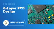
Once you’ve run out of room on your 4-layer PCB, it’s time to graduate to a 6-layer board. The additional layer can give you room for more signals, an additional plane pair, or a mix of conductors. How you use these extra layers is less important than how you arrange them in the PCB stackup, as well as how you route on a 6-layer PCB. If you’ve never used a 6-layer board before, or you’ve had EMI troubles with this stackup that are difficult to solve, keep reading to see some 6-layer PCB design guidelines and best practices.
Blog
•
Altium Designer 22.5 Update
We are happy to announce that the Altium Designer 22.5 update is now available. Altium Designer 22.5 continues to focus on improving the user experience, as well as performance and stability of the software, based on feedback from our users. Check out the key new features in the What's New section on the left side of this window!

Blog
•
How Reliable is Your Hybrid PCB Stackup?
PCB stackups often incorporate slightly dissimilar materials that could pose a reliability problem. Hybrid PCBs are one case where the PCB stackup will include different materials, typically a standard FR4 laminate and a PTFE laminate for RF PCBs. Designers who want to take the lead on material selection when designing their hybrid stackups should consider these factors that affect reliability. As with any PCB stackup, make sure you get your fabricator involved in the manufacturing process early to ensure reliability problems do not arise during production.

Blog
•
Is it Simultaneous Switching Noise or Crosstalk?
Going deeper into crosstalk, there is always the issue of verifying EMI/EMC compliance through test and measurement. With the multitude of signal integrity problems that can arise in real PCBs, how can the astute designer distinguish them all? Some problems are clearer than others, with specific signal integrity measurements being developed for testing and measuring particular aspects of signal behavior. The fact is, multiple signal integrity problems could be present on a single interconnect simultaneously.

Blog
•
Sharing PCB Data with Manufacturers in the Cloud
Once you’ve finished your new project and you’re ready to push it to your manufacturer, you’ll normally be stuck in an endless email chain with an engineer, or you’ll have to share cloud links with each other. The cloud sharing and design release tools in Altium Designer and Altium Concord Pro are a huge help in this area. In this post, I’m going to take an existing project I’ve worked with in a number of recent blogs, create some fabrication and assembly documentation, and finally push this data to a manufacturer using Altium Concord Pro.

Blog
•
The Great PCB Layout "Rules of Thumb" Debate Rages On
To this day, I still see many PCB layout “rules of thumb” that first became common nearly 20 years ago. Do these rules still universally apply? The answer is a firm “maybe.” The discussion around PCB layout rules of thumb is not that these rules are correct or incorrect. The problem is that the discussion around these rules often lacks context, leading to the always/never type of discussion seen in some popular forums. My goal in this article is to communicate the context behind the common PCB design rules.
Blog
•
How to Design Your PCB Test Coupon and What You Can Test
As the operating speed of components has increased, controlled impedance is becoming more common in digital, analog, and mixed-signal systems. If the controlled impedance value for an interconnect is incorrect, it can be very difficult to identify this problem during an in-circuit test. However, testing is normally performed on a PCB test coupon, which is manufactured on the same panel as the PCB. If you want to get through board spins quickly and aid future designs, you might consider designing a test coupon and keeping it handy for future designs.

Blog
•
Altium DbLibs and Electronic Components in the Cloud with Altium Designer 20.1
Altium’s DbLib support is one of the oldest and most loved features of Altium Designer for managing electronic components and their data. They’ve been present in the software world since before I could fathom the existence of Ohm’s law. Altium 20.1’s new Component Sync feature allows you to synchronize virtually any database or database Library with Altium 365, taking advantage of both approaches strengths.
Blog
•
What is a Schematic Netlist for Your PCB?
If you’ve created your next great schematic, there is a lot going on behind the scenes in your design software. A schematic netlist is one of the central pieces of information that will be used in multiple features in your design software to create a real PCB. Your schematic netlist provides both electrical connectivity information, and reflects the functional structure of your design data in a single set of data.
Blog
•
How to Select an Inductor for a Buck Converter
An SMPS is one of those quiet (yet electrically noisy) devices that makes your favorite electronics run smoothly. Among the numerous DC-DC converter topologies, a buck converter finds plenty of uses for stepping down the input voltage to a lower level while providing high efficiency power conversion. A common question around component selection for these power converters is how to select an inductor for a buck converter. The goal in working with an inductor and other components in a buck converter is to limit power loss to heat and while minimizing current ripple.

Blog
•
US Department of Transportation Seeking Alternatives to GPS
GPS-capable devices range from your phone to your smartwatch; simply type in your destination and follow the directions. Simple, right? According to the Washington Post, we should all stop using GPS as it’s ruining the navigation centers of our brains. Despite the neurological effects on perception and judgment, the U.S. Department of Transportation (DOT) aims to find alternatives to GPS to provide redundancy.

Blog
•
Bluetooth 5.1 SoC vs. Module: Which is Best for Your Design?
The list of features available in Bluetooth just got a little longer since the release of Bluetooth 5.1. If you want to incorporate a Bluetooth 5.1 SoC into your new product, you have two primary options for bringing this component into your board. The first is as an SoC that mounts to your board just like any other component. The other option is to bring a module into your new board—directly onto the surface layer. Here’s what you need to know about a Bluetooth 5.1 SoC or module in your next IoT product.
Blog
•
Altium 365 Getting Started User Guide - Available Now
Get Started with Altium 365 with a step-by-step guide and videos to experience the most connected experience for PCB design and realization: https://my.altium.com/altium-365/getting-started/

Blog
•
USB Power Delivery for Your Next Project
Since its introduction in the late 90s, the USB standard has never ceased to grow in popularity. There has been a growing trend toward USB being a power delivery interface with data, rather than a data interface that can supply power, as the 1.0 specification originally intended. To supply the increasing thirst for power over USB, the USB 3.0 Spec with Type-C began implementing the Power Delivery standard, which you should consider using for your next electronics project.
Blog
•
Circuit Board Design for In-Circuit Testing
There are many types of circuit board tests available in electronics manufacturing today, each having unique goals and characteristics. This article presents guidelines at the design level (schematic and layout) to enable the use of in-circuit testing (ICT) fixtures to verify proper component assembly. These simple test fixtures allow your board to be tested as its assembled, which helps identify and remove failed boards from your production run.

Blog
•
Planning for the Future with Cirris Systems and Altium
Technological advancements have been a hallmark of the past few decades, from the widespread adoption of internet technology to the smartphones and wireless devices we rely on every day to stay connected. Orlan Thatcher, Board Layout Specialist at Cirris Systems, could never have predicted the demand their services would generate. The company struggled with six different software platforms before switching to Altium Designer.

Blog
•
An Introduction to NFC
I used to work in a research lab that worked primarily with RFID (Radio Frequency IDentification) and NFC (Near Field Communication) technology, particularly for the agriculture industry and cattle identification. These were very specialized fields; however, the lab also worked on projects which involved retail and various other applications for NFC. It’s an amazing technology that you might be using every day without thinking about it - building access to your mobile phone payments, for instance.

Blog
•
Editing Your PCB Geometry with MCAD Tools
You need to define your PCB geometry in the context of your enclosure. If your board cannot physically be assembled into the final product, it doesn't matter how well laid out it is electrically. This webinar focuses on how the MCAD CoDesigner allows you to edit your PCB in the context of a higher-level assembly, allowing you to respect the relevant mechanical constraints.
Blog
•
The PCB Fabrication Process — what Every Design Engineer Needs To Know, Part 2
In Part 1 of this article, I described the first steps that occur during the PCB fabrication process. They detailed the inner layer processing effort as well as the efforts that take place during the transition from inner layer processing to lamination. This part of the article will provide a detailed description of the lamination, drilling and plating processes.
















Your search returns no results.


