Welcome, Guest

Sign in to learn, create, and do more with the product you love.

News & Updates

Filters:
Tag
Embedded thumbnail for Assuring Your Board Is Large Enough to House All Components
How-To's
Assuring Your Board Is Large Enough to House All Components

This video covers how to make sure your board is big enough to house all your components.

Blog
Altium Designer 22.8 Update

We are happy to announce that the Altium Designer 22.8 update is now available. Altium Designer 22.8 continues to focus on improving the user experience, as well as performance and stability of the software, based on feedback from our users. Check out the key new features in the What's New section on the left side of this window!

What is Hybrid Beamforming?
Blog
What is Hybrid Beamforming?

In this article, we’ll look at beamforming implementation in an advanced method combining analog and digital techniques, known as hybrid beamforming. This method blends both digital and analog techniques to create multiple beams and thus reach multiple users with varying intensities. In the case of an RF imaging system or a radar system, hybrid beamforming in a MIMO technique also allows tracking of multiple targets with adjustable resolution.

Article preview
On-Demand Webinar
PCB Design in Altium Designer with Differential Data Transfer

Differential data transmission lines usage can be challenging for even experienced designers. First you need to be familiar with the concepts of differential data transmission, find out why it is used, and what the potential advantage for your signal. This webinar will help you determine what part of your designs need differential pairs implementations and how to create such pairs with a given wave impedance in Altium Designer.

Is your via impedance calculator accurate?
Blog
Why Most Via Impedance Calculators Are Inaccurate

The problem with every via impedance calculator that I have seen is simple: they are incomplete or totally wrong. The “incomplete” part refers to a lack of context; these calculators can roughly reproduce a well-known estimate from a legend like Howard Johnson in his Digital Design textbooks. However, these calculators never provide insight into what they are actually calculating, or where the calculated via impedance is accurate. Keep reading to see why these calculators get it so wrong, as well as the context surrounding via impedance.

Embedded thumbnail for How to Create an Interactive PDF of a Schematic Diagram
How-To's
How to Create an Interactive PDF of a Schematic Diagram

This video shows how to create an interactive PDF using the Smart PDF Wizard.

Embedded thumbnail for What is the Draftsman Document?
How to Work with Draftsman
What is the Draftsman Document?

Once your PCB layout is finished it’s time for review. This is where the Draftsman Document and Altium Designer’s Draftsman Editor comes in.

Blog
Buck Converter Simulation in Altium Designer

When designing high power circuits (usually very high voltage and/or current), you’ll need to create a regulator from scratch and place it in your PCB layout. It's also the case that you may want to model a real component using discretes in a simulation in order to qualify the system's expected operating regime. As part of buck converter design, you can easily run a buck converter simulation directly in Altium Designer’s schematic editor. Here’s how you can access these features in the newest version of Altium Designer. 

Embedded thumbnail for Adding Project Modules to a Multi-board Schematic
How to work with Multiboard
Adding Project Modules to a Multi-board Schematic

If you’re using multiple PCBs in your Multi-board design, Altium Designer allows you to add existing projects directly to your schematic with modules. We’ll show you how to quickly and efficiently add these projects to your Multi-board design.

PCIe 6.0 Overview
Blog
Overview of the PCIe 6.0 Standard

Just as you get used to PCIe 5.0, they decide to release another standard! The newest iteration of PCIe is Gen6, or PCIe 6.0. PCIe 6.0 brings a doubling of channel bandwidth through introduction of PAM-4 as the signaling method in high-speed differential channels. This signaling method is a first for PCIe, and it’s an important enabler of the doubled data rate we see in the current standard. In this article, I’ll run over the important points in the standard and what PCB designers can expect when designing these channels.

Embedded thumbnail for Checking for Creepage in High Voltage Designs
How-To's
Checking for Creepage in High Voltage Designs

High voltage devices have leakage currents that propage over the surface of the board. In such devices, it's important to consider not only the standard gap between the two topological elements, but also the shortest possible path between them, taking into account cut-outs and holes. With Altium Designer 20, you can check for creepage using the new creepage distance rule.

Embedded thumbnail for Creating BGA Footprints with the Footprint Wizard
How to create a PCB Footprint
Creating BGA Footprints with the Footprint Wizard

Altium Designer makes it easy to create a BGA footprint using our IPC compliant footprint wizard. We'll show you how easily you can create and modify a BGA footprint using the footprint wizard.

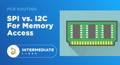
SPI vs. I2C For Memory Access
Blog
SPI vs. I2C: How to Choose the Best Protocol for Your Memory Chips

One of the common implementations of SPI and I2C in a PCB layout is as a protocol for reading and writing to an external Flash memory. Flash chips are a very common component in embedded systems and can offer high capacities of non-volatile memory up to Gb values. When choosing a memory chip, you'll want to match the application requirements and functionality with the bus speed you need for read and write operations in your memory chip. There is also the matter of the type of Flash memory you'll need to access (NOR vs. NAND).
On-Demand Webinar
Tips & Tricks: Board Shape Creation

Being able to design a board in your ECAD environment doesn’t mean that it is manufacturable in real life. You have to make sure your CAD representation won’t have any problems in the real world by taking some precautions. For example, there are certain areas that need to be free of components and have specified clearances like your board edge. This webinar will help you get acquainted with the creation and modification of your board shape so that you can ensure manufacturability.

Blog
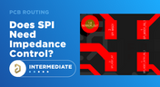
Is There an SPI Trace Impedance Requirement?

There is no SPI trace impedance requirement? The reality is that SPI lines only start to need impedance control when the length of the interconnect becomes very long. And because there is no specific impedance requirement in the bus, you have some freedom in channel design and termination. So what exactly qualifies as “very long” and when is some termination method needed? We’ll break it down in this article.

Embedded thumbnail for How to Remove Unused Pad Shapes
How-To's
How to Remove Unused Pad Shapes

Unused pad shapes can cause distortion among other problems so it is best to exclude them from your designs. This video shows how to remove unused pad shapes.

Embedded thumbnail for Stackup Presets and Templates
How to work with Layer Stack Manager
Stackup Presets and Templates

In this video, we will learn how to apply predefined layer stacks to the board, as well as how to save the layer stack file as a template.

The Skin Effect and EM Fields
Blog
The Skin Effect, Current Density, and the Electromagnetic Field

During this year's AltiumLive CONNECT event, I recall receiving an interesting question about the skin effect and the distribution of current due to the presence of ground in coplanar transmission lines. In this article, we'll look at the electric field around a transmission line carrying a signal, and how this might be impacted by the skin effect.

Embedded thumbnail for Creating a PCB Footprint Assembly Drawing
How to create a PCB Footprint
Creating a PCB Footprint Assembly Drawing

If you need to create an assembly drawing of your PCB Footprint for your outjob files we can show you how in Altium Designer. We’ll walk through all the different options for your assembly drawing in your Draftsman document, how to create your assembly drawing and assign it designators.

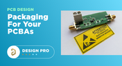
Packaging for your PCBAs
Blog
What You Need for PCB Packaging and Shipping

When you get your PCBA back from an assembler, you’ll notice the packaging materials used to pack and ship the PCBA. Those materials are specific to electronics, and if you build products on behalf of clients, it’s important to know the packaging materials used for packing and shipping electronics. In this article I’ll show the main set of materials and equipment used to package electronics assemblies.

Tag
Schematic Compare
Blog
Schematic Compare

A design project doesn’t appear out of nowhere. The design process spreads over time, and project documents change. Schematic documents gradually become more complex, new functional blocks appear, and already finished parts can be modified and updated.

Embedded Capacitance Materials Overview
Blog
Embedded Capacitance Materials Overview

Capacitance is your friend whenever you need stable power integrity, which is why there is so much focus on decoupling capacitors. While these components are important and they can be used to provide targeted power integrity solutions to certain components, there is one specialty material used to supercharge capacitance in your PCB stackup or package substrate. 

How To Import Libraries and Manage Components With Altium 365
Blog
How To Import Libraries and Manage Components With Altium 365

The problems you can experience with components and libraries are endless. These problems are the most significant source of design issues and the biggest reason behind respins, costing companies untold amounts of lost profit annually.
If you want to have a better understanding of how to use Altium 365 to maintain a strong and centralized library that is free of problems and headaches, you may want to consider attending this lecture.

The High-Speed PCB Stackup Design Challenge
Blog
The High-Speed PCB Stackup Design Challenge

As much as we would like to build every high speed PCB perfectly, with ideal SI/PI/EMI characteristics, it isn’t always possible due to many practical constraints. Sometimes a stackup can be “good enough,” even for a high-speed PCB. This always comes from the need to balance engineering constraints, functional requirements, and the need to ensure signal and power integrity in a high-speed design, and finally to ensure compliance with EMC requirements.

How I Improved My Collaboration Efficiency with Altium 365
Blog
How I Improved My Collaboration Efficiency with Altium 365

Involving the whole team that will bring a product to completion early on in the development cycle is vital to efficient development. Design reviews with all the relevant parties are critical at each step of the design process, starting with high-level component selection, then through the schematic capture and PCB layout stages. 

Countersink and Counterbore
Blog
Countersink and Counterbore

Ergonomics and convenience are important issues when designing a printed circuit board and the device as a whole. A lot of Altium Designer tools are aimed at solving them. These include Countersink and Counterbore holes, which allow the use of various types of screws in the mounting holes of the board.

Migrating Data From Other Version Control Systems
Blog
Migrating Data From Other Version Control Systems

The development of electronic devices always involves the release of many different types of files. And these files are not static - they change as the project progresses. When filling a project with data, a user creates new files, modifies outdated files that have become irrelevant. Managing project data is a separate task, especially for large developments where several participants with different specializations are involved in the process.

Properties Panel Tuning
Blog
Properties Panel Tuning

High-speed PCBs often require tuning groups of tracks, both single and differential. Altium Designer includes powerful tools that allow you to solve such tasks quickly and with high quality. Study this document and achieve the desired result even faster.

Reflectionless Matching vs. Conjugate Matching: An Apparent Contradiction
Blog
Reflectionless Matching vs. Conjugate Matching: An Apparent Contradiction

There is one confusion related to impedance matching that comes up again and again, and it appears to be a fundamental confusion between reflection and power delivery. This leads to an apparent contradiction that arises when we try to generalize power delivery to wave reflection, despite the fact that the two were not meant to be related.

Properties Panel Routing
Blog
Properties Panel Routing

Routing is one of the most time-consuming stages of PCB design. Altium Designer has a large set of tools that allow you to do it as accurately and quickly as possible. This document will help you to learn how to manage your routing effectively and use it to its fullest extent.

Quarter-Wave Transformer Design For Real and Reactive Loads
Blog
Quarter-Wave Transformer Design For Real and Reactive Loads

RF systems operate with specific impedance values across entire interconnects, including on PCBs. Not all RF components are packaged in integrated circuits with defined impedances, so impedance matching circuits and line sections are needed to ensure signal transmission between different sections of an interconnect. One of these impedance matching techniques is the quarter-wave impedance transformer, which can be implemented as a printed trace with specific impedance.

Schematic
Blog
Altium Designer 22.10 Update

We are happy to announce that the Altium Designer 22.10 update is now available. Altium Designer 22.10 continues to focus on improving the user experience, as well as performance and stability of the software, based on feedback from our users. Check out the key new features in the What's New section on the left side of this window!


Component Warpage Causes in a PCB
Blog
Component Warpage Causes in a PCB

A staff member at a PCB manufacturer once explained to me that they thought we were having an issue with a package warping. Unfortunately, component warping can occur both in a PCB and in components. In this article, we'll give an overview of warpage in a PCB, specifically in the circuit board and in the components.

Link Budget Calculator
Blog
RF Signal Chain and Link Budget Basics

If you're designing a wireless IoT device, and you know how to calculate the link budget, you can reasonably estimate whether your signal will reach its destination and be read by the receiver. To calculate the link budget, the designer needs to know something about all other sources of gain and loss in the system. Once link budget is determined, the designer can judge whether some modification is needed in their RF signal chain. 

How to Calculate SMD Pad Sizes?
Blog
Best Methods for Calculating SMD Pad Size in PCB Design

SMD components require precisely sized pads for soldering during assembly. The designer is responsible for ensuring pad sizes are correct, either by calculating them and comparing with footprint data, looking through datasheets, or by memorizing SMD pad size standards. If you have a component and you don't have access to the footprint, and you decide to biuld the footprint yourself, what resources are available to ensure you have the correct pad size?

Can You Fix a Warped PCB?
Blog
Can You Fix a Warped PCB?

Before we get too deep into this article, I’ll give you the simple answer. You probably can’t fix warping in your PCB after it’s already been fabricated. You can prevent an unwarped board from becoming warped during assembly, but only as long as materials were selected properly and the board is put into reflow correctly. We’ll run over some of these points in this article, and I’ll examine some points that might help you recover a warped board.

Tag
NEW
Embedded thumbnail for Skip Layer Routing for RF: Control Impedance & Cut Insertion Loss
How-To's
Skip Layer Routing for RF: Control Impedance & Cut Insertion Loss

Discover our latest video and learn how RF designers use a deeper ground plane to minimize skin-effect resistance, improve signal integrity over long high-frequency routes, and optimize impedance matching for oversized SMT pads in antenna launches and coaxial connectors.

NEW
Embedded thumbnail for Just Released: ODB++ Intellectual Property Protection
New in Altium's Software
Just Released: ODB++ Intellectual Property Protection

ODB++ Intellectual Property Protection lets you control exactly what design data is included in the ODB++ output, ensuring each manufacturing partner receives only the information needed for their specific fabrication or assembly tasks.

Embedded thumbnail for Future of Electronics Development in Security and Aerospace
How-To's
Future of Electronics Development in Security and Aerospace

See the highlights from Altium's executive event in Hamburg, where Security and Aerospace leaders explored AI-driven development, digital engineering, supply chain resilience, and the future of mission-critical electronics.

Embedded thumbnail for Create Clearance Rules Faster and with Less Effort
New in Altium's Software
Create Clearance Rules Faster and with Less Effort

Setting up clearance rules is now more intuitive in the Constraint Manager. Choose the Simple view for faster configuration with grouped object types, or the Advanced view when you need detailed, matrix-based clearance control.

Embedded thumbnail for Mastering HDI Design Rules in Altium Designer
How-To's
Mastering HDI Design Rules in Altium Designer

In our latest Altium Academy tutorial, we guide you through configuring the essential HDI PCB design rules in Altium's software. You'll learn how to use your manufacturer's fabrication capabilities to create accurate design rules and constraints for your PCB.

Embedded thumbnail for Search, Filter, and Navigate PCB Designs Faster
New in Altium's Software
Search, Filter, and Navigate PCB Designs Faster

The Web Viewer now features a redesigned search experience for faster access to PCB design data across supported CAD formats. A lightweight, intuitive interface lets you begin with simple search terms and progressively refine results using contextual suggestions.

Embedded thumbnail for Gain Better Control Over Wire Bond Visibility
New in Altium's Software
Gain Better Control Over Wire Bond Visibility

New bond wire visibility controls give you greater flexibility when working with wire-bonded boards and footprints, making it easier to focus on the details that matter most.

Embedded thumbnail for Coming Soon: Selectable Harness Source Within Multi-board Design
New in Altium's Software
Coming Soon: Selectable Harness Source Within Multi-board Design

Selectable Harness Source Within Multi-board Design enables harness projects to drive system connectivity while maintaining bidirectional synchronization between multi-board schematics and harness wiring diagrams for improved accuracy and easier design management.

Embedded thumbnail for Choose the Simbeor Version for Your PCB Calculations
New in Altium's Software
Choose the Simbeor Version for Your PCB Calculations

The PCB Editor now lets you choose the Simbeor version used for delay and impedance calculations, giving you more flexibility and consistency across your design workflows.

Embedded thumbnail for Improve PCB Editor Performance with Via Instancing
New in Altium's Software
Improve PCB Editor Performance with Via Instancing

The PCB Editor now uses via instancing to generate geometry for each via individually, providing greater flexibility and a more advanced approach to managing vias in PCB designs.

Embedded thumbnail for GSSG Stackup Deep Dive: Routing, Impedance, and HDI
How-To's
GSSG Stackup Deep Dive: Routing, Impedance, and HDI

A ground-signal-signal-ground (GSSG) stackup rethinks the traditional four-layer PCB structure by moving the ground planes to the outer layers and routing signals on the two inner layers. In this Altium Academy deep dive, we review a real one-minute design review submission and demonstrate how to configure a GSSG stackup properly using the Layer Stack Manager.

Embedded thumbnail for Generate IPC-7351B Compliant Footprints with More Control
New in Altium's Software
Generate IPC-7351B Compliant Footprints with More Control

The IPC Compliant Footprint Wizard has been updated to improve IPC-7351B compliance across supported package types. Enhancements include footprint calculations, package outlines, silkscreen and courtyard generation, layer mapping, density table behavior, and new pad trimming controls for gullwing packages, with support added to the batch generator Excel template.

Embedded thumbnail for Add Unit-Aware Temperature Coefficient Parameters
New in Altium's Software
Add Unit-Aware Temperature Coefficient Parameters

Component templates in a connected Workspace on the Altium Platform now include support for Temperature Coefficient (ppm/°C) as a unit-aware user parameter type. This makes it possible to define temperature coefficient values directly within the template using the appropriate units.

Embedded thumbnail for When to Add Part Numbers to SMD Passives
How-To's
When to Add Part Numbers to SMD Passives

Check out our new video covering essential electronics fundamentals, with a focus on why including part numbers for SMD passive components, such as SMD resistors, directly on schematics is so important. We also explore whether relying only on the Bill of Materials (BOM) is enough for effective electronic component management.

Embedded thumbnail for Present Large Harness Tables More Clearly
New in Altium's Software
Present Large Harness Tables More Clearly

Harness Draftsman now supports splitting connection tables across multiple pages in *.HarDwf documents. With the new page height limit setting, you can easily control how much of the table appears on each page.

Embedded thumbnail for Innovate Beyond - The Future of Electronics Development in Automotive
How-To's
Innovate Beyond - The Future of Electronics Development in Automotive

Discover how the future of automotive electronics is being shaped by a more connected development approach that unifies teams, data, requirements, design, collaboration, and manufacturing. Recorded at BMW Welt and the BMW Museum during Altium’s "The Future of Electronics Development in Automotive" event, this video explores the key challenges and innovations driving the next generation of automotive design.

Tag
Your search returns no results.