News & Updates


Blog
•
Behind the Scenes with AI Embedded Development
Forget one-shot AI hacks Ari Mahpour shows the thoughtful, sustainable way to integrate AI into embedded firmware development. Learn the core principles (planning gate, HAL abstraction, observability, timeout design) that can help you push your efficiency 5-10 times in real hardware projects.


Blog
•
We're heading to PCB West 2025!
Join Altium at PCB West 2025 in Santa Clara, CA, on October 1! Stop by Booth 300 for the official launch of the new Altium platform, built on the foundation of Altium Designer and Altium 365. Be sure to check out our live demos of Altium Develop and Altium Agile.

Blog
•
Peak Electrical Performance in Multi-Board Designs With Advanced Simulation and Compliance Tools
Moving from single-board to multi-board systems is a leap in complexity. You must manage not just routing, but power, signal integrity, mechanical fit, and regulatory requirements across boards. In this article, you’ll discover how Altium’s advanced simulation and compliance tools help engineering teams overcome these challenges and deliver reliable multi-board solutions.

Blog
•
How to Catch Enclosure and Connector Misalignment Before the First Prototype
As electronics continue to miniaturize and functionality increases, even minor misalignments between enclosures and connectors can derail a project. This article explores how early integration of ECAD and MCAD workflows helps detect and eliminate those costly issues before the first prototype is built.


Blog
•
Executive Insights Into Electronic Product Development Gaps You Need To Close
Electronics hardware development is falling behind broader product development disciplines due to fragmented workflows, poor collaboration, and limited compliance visibility. This gap introduces risk, delays, and missed opportunities but executives see real business value in modernizing electronics development through better integration, traceability, and lifecycle visibility.


Blog
•
Sourcing For High-Mix Low-Volume Electronics Manufacturing
High-mix, low-volume (HMLV) electronics manufacturing requires agile sourcing strategies to handle shifting BOMs, erratic lead times, and component volatility. All while controlling costs and ensuring compliance. Cloud-based tools like Altium provide real-time component visibility, BOM collaboration, and supplier integrations to help navigate HMLV complexities.


Blog
•
How to Solve Fit, Form, and Function Challenges in Robotics with ECAD-MCAD Collaboration
As robotics systems become increasingly miniaturized and intricate, ensuring perfect fit, form, and function across electrical and mechanical domains is critical to avoid design setbacks. Real-time ECAD-MCAD integration with two-way sync empowers teams to streamline workflows, reduce PCB rework, and deliver more reliable designs faster.


Blog
•
One Vision, Three Powerful Solutions: Introducing Octopart Discover, Altium Develop, and Altium Agile
We are excited to announce the launch of three new platform-based solutions that will transform the way electronic products are designed, built, and delivered: Octopart Discover, Altium Develop, and Altium Agile. These solutions are designed to simplify processes, accelerate innovation, and make collaboration seamless across the entire electronics lifecycle. Together, they realize the purpose of Altium and Renesas: To Make Our Lives Easier.

Blog
•
The Cost of Overreaction: How Misguided Orders Disrupt the Semiconductor Market
Discover how short-sighted ordering practices fuel volatility in the semiconductor market and why smarter, data-driven approaches are key to building resilience and sustainability.


Blog
•
The Top 5 Workflow Bottlenecks Slowing Down Mechanical Engineering Teams
Mechanical engineering teams frequently encounter delays from fragmented communication, disconnected toolchains, and inefficient synchronization processes. This article examines five critical workflow bottlenecks and highlights how ECAD-MCAD integration with real-time, bidirectional updates can eliminate rework and accelerate design iterations.

Blog
•
Optimize Your Multiboard PCB System with Intelligent Design and Manufacturing Solutions
Optimizing multiboard PCB systems demands visibility across logical, physical, and manufacturing domains. This article outlines how Altium’s environment lets engineers establish system‑level schematics, 3D spatial validation, harness documentation, and synchronized outputs to streamline design and production.
Blog
•
RF Power Supply Design and Layout Guide
One thing is certain: power supply designs can get much more complex than simply routing DC power lines to your components. RF power supply designs require special care to ensure they will function without transferring excessive noise between portions of the system, something that is made more difficult due to the high power levels involved. In addition to careful layout, circuitry needs to be designed such that the system provides highly efficient power conversion and delivery to each subsection of the system.
Blog
•
Methods to Protect your Circuit
Overvoltage, overcurrent, and heat are the three most likely events that can destroy our expensive silicon-based components or reduce our product’s life expectancy. The effects are often quite instant, but our product might survive several months of chronic overstress before giving up the ghost in some cases. Without adequate protection, our circuit can be vulnerable to damage, so what should we do? Or do we need to do anything?

Blog
•
SUBCKT Sharing: The Fastest Ways to Share SPICE Models Online
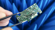
Today’s PCB designers and layout engineers often need to put on their simulation hat to learn more about the products they build. When you need to perform simulations, you need models for components, and simulation models often need to be shared with other team members at the project level or component level. What’s the best way for Altium Designer users to share this data? Read this article to learn more about sharing your models with other design participants.
Blog
•
RF PCB Material Comparison for mmWave Devices
When some designers start talking materials, they probably default to FR4 laminates. The reality is there are many FR4 materials, each with relatively similar structure and a range of material property values. Designs on FR4 are quite different from those encountered at the low GHz range and mmWave frequencies. So what exactly changes at high frequencies, and what makes these materials different? To see just what makes a specific laminate useful as an RF PCB material, take a look at our guide below.

Blog
•
Low Cost Solutions for Automated Hardware in the Loop Testing
In today’s fast-paced world where iterations of electronics are spun at lightning speeds, we often forget one of the most critical aspects of development: testing. Even if we have that fancy test team, are we really able to utilize them for every modification, every small and insignificant change that we make to our prototypes? In this article, we will review a very low cost, yet highly effective and quite exhaustive test system that will get you that bang for your buck that you’ve been looking for.

Blog
•
Best Practices for Using DNI/DNP Entries in Your PCB BOM
If you’ve ever looked at the BOM for a reference design or an open-source project, you may have seen a comment in some of the entries in your BOM. This comment is either “DNP” or “DNI”. If you think about it, every component placed in the PCB requires some level of placement and routing effort, which takes time and money if you’re working for a client. This begs the question, why would anyone design a board with components they don’t plan to include in the final assembly?
Blog
•
Altium OutJob Files vs. Project Release: What's the Difference?
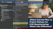
When it’s time to share your design data with your manufacturer, it’s like taking a leap of faith. Sending off a complete documentation package might seem as easy as placing your fab files in a zip folder, but there are better ways to ensure your manufacturer understands your project and has access to all your design data. For Altium Designer users, there are multiple options for creating and packaging release data into a complete package for your manufacturers.
Blog
•
Testing the Limits of Your LDO's Efficiency
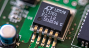
If you’re designing a circuit board to be powered by anything except a bench-top regulated power supply, you’ll need to select a power regulator to place on your board. Just like any other component, your regulator has stated operating specs you’ll see in a product summary, and it has more detailed specs you’ll find in a datasheet. The fine details in your datasheets are easy to overlook, but they are the major factors that determine how your component will interact with the rest of your system.

Blog
•
How Total Harmonic Distortion Affects Your Power System
It would be nice if the power that came from the wall was truly noise-free. Unfortunately, this is not the case, and although a power system can appear to output a clean sine wave, zooming into an oscilloscope trace or using an FFT will tell you a different story. When you take "dirty" power, put it through rectification, and then pass it through a switching regulator, you introduce additional noise into the system that further degrades power quality. If you’re a power supply or power systems designer, then you know the value of supplying your devices with clean, noise-free power.
Blog
•
What PCB Copper Thickness Should You Use?
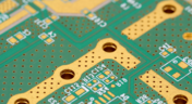
If you’re an electronics designer or you’re just beginning your career as an engineer, the PCB stackup is probably one of the last things you’ll think about. Simple items like PCB copper thickness and board thickness can get pushed to the back burner, but you’ll need to think about these two points for many applications as not every board will be fabricated on a standard 1.57 mm two-layer PCB
Blog
•
Should You Route Signals in Your PCB Power Plane?
I often get questions from designers asking about things like signal integrity and power integrity, and this most recent question forced me to think about some basic routing practices near planes and copper pour. "Is it okay to route signal traces on the same layer as power planes? I’ve seen some stackup guidelines that suggest this is fine, but no one provides solid advice." Once again, we have a great example of a long-standing design guideline without enough context.

Blog
•
The Anatomy of Your Schematic Netlist, Ports, and Net Names
Electronics schematics form the foundation of your design data, and the rest of your design documents will build off of your schematic. If you’ve ever worked through a design and made changes to the schematic, then you’re probably aware of the synchronization you need to maintain with the PCB layout. At the center of it all is an important set of data about your components: your schematic netlist. What’s important for designers is to know how the netlist defines connections between different components and schematics in a large project.

Blog
•
How to Compare PCB Manufacturing Services for Your Board
There are plenty of PCB manufacturing services you can find online, and they can all start to blend together. If you’re searching for a new service provider, it can be hard to compare all of them and find the best manufacturer that meets your needs. While experienced designers can spot bogus manufacturers from afar, there is always a temptation to go with the lowest priced, supposedly fastest overseas company you can find. However, there is a lot more that should go into choosing a PCB manufacturing service than just price.

Blog
•
Pi Filter Designs for Power Supplies
Pi Filters are a type of passive filter that gets its name from the arrangement of the three constituent components in the shape of the Greek letter Pi (π). Pi filters can be designed as either low pass or high pass filters, depending on the components used. The low-pass filter used for power supply filtering is formed from an inductor in series between the input and output with two capacitors, one across the input and the other across the output. Keep reading to learn more about their application in the PCB Design.
Blog
•
How to Design a Hybrid PCB Stackup
The first question that should come up when selecting materials and planning a stackup is: what materials are needed and how many layers should be used? Assuming you’ve determined you need a low-loss laminate and you’ve determined your required layer count, it’s time to consider whether you should use a hybrid stackup. There are a few broad situations where you could consider using a hybrid stackup with low-loss laminates in your PCB

Blog
•
Efficient Battery Power Supplies
Batteries offer a great power source for electrical devices that need to be mobile or located somewhere where connection to a mains electricity supply or other power source is impossible. The biggest problem with battery power is the expectation of users that the device will operate for significant periods with the need for recharging or replacing the batteries. This demand is placing the onus on the designer to improve efficiency and reduce power demand to meet this need.
















Your search returns no results.


