News & Updates
Blog
•
Getting Through PCB DFM
In this article, we’ll discuss the key design features to implement, and steps to take prior to fabrication that will help prevent some DFM process pain.
Blog
•
Level Up Your Design Skills - Altium Designer Getting Started User Guide Update
We are happy to announce the new update of our Altium Designer Getting Started User Guide. Whether you are new to Altium Designer or you want to brush up on some topics, the Altium Designer Getting Started User Guide will take you from a beginner to a master in PCB design.
This is only the beginning! This guide will be updated with new information based on user feedback. Let’s first go over the contents of the guide.


Blog
•
Modeling Copper Foil Roughness in Altium Designer's Impedance Profiler
With the new layer stack manager in Altium Designer®, you can now include copper foil roughness factors directly in your impedance calculator. This is quite easy to do in the layer stack manager, but it begs the question: what exactly is the copper roughness factor? Which value should be used for your interconnects?


Blog
•
High-Speed Signal Routing: The 5 Important Constraints
After you capture your schematic as an initial layout and create an initial component arrangement, it’s time to define your routing constraints. Doing this early will allow your DRC engine to spot rules violations before you finish your layout. Likewise, you’ll be able to modify the default rule set to meet your layout requirements. Here are the important routing constraints you’ll need to check before you start routing your board.
Blog
•
CoDesigner and MCAD Component Placement On-Demand Webinar
Learn how to place components from the MCAD side and synchronize them with Altium Designer ECAD models, designators, and sourcing data to simplify your design process.
Blog
•
How to Create a PCB Manufacturing Cost Estimation
Some manufacturers have very convenient PCB manufacturing cost estimation calculators you can use, but the real costs depend on a number of factors. If you’re an entrepreneur and you’re producing your own boards, or you are managing manufacturing, testing, and delivery for a new project, it’s your job to help clients understand the primary cost drivers for new boards. Here’s how you can get an estimate of your fabrication costs, both for local and overseas manufacturers.

Blog
•
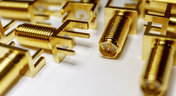
PCB Mountable Connectors: SMD vs. Through-hole
Selecting a connector is as much an art as it is a science. The artistic side is all about aesthetics and satisfying clearances, while the scientific side is all about signal integrity. For PCB mountable connectors, you’ll need to choose between surface-mounted or through-hole connectors, and you’ll need to consider how each type affects signal integrity in your application. Here’s what you need to think about beyond the standard connector specifications.

Blog
•
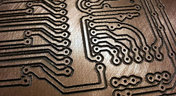
PCB Via Current-Carrying Capacity: How Hot is Too Hot?
Trace and via current-carrying capacity are legitimate design points to focus on when designing a new board that will carry high current. The goal is to keep conductor temperatures below some appropriate limit, which then helps keep components on the board cool.
Blog
•
How to Maximize Copper in Your PCB Design: The Pros and Cons of Copper Pouring Versus Placing
There is a saying in copper pour PCB design, “Copper is free.” It means a PCB editor designer must think in reverse. A board starts off as solid copper, and the copper you don’t want is removed. It is faster to build, less consumptive, and less expensive to make a board that is mostly copper as compared to the same size board that is mostly bare. Picking the correct technique will make the difference between an effortless or frustrating experience.


Blog
•
Top 5 PCB Design Guidelines Every PCB Designer Needs to Know
What’s the key to designing a board that’s realistic on paper and in physical form? Let’s explore the top 5 design guidelines that you need to know to design your next manufacturable, functional and reliable PCB.

Blog
•
May 14, 2020
How to Highlight Nets in Altium Designer to Simplify Schematic and PCB Designs
Highlighting nets will help you simplify your schematic and PCB design. In Altium , there are multiple options that enable you to leverage this capability to simplify the verification of connections and circuit paths and make sure that the design you send to your manufacturer accurately reflects the printed circuit board you need built.

Blog
•
May 12, 2020
Keep Your Altium Designer PCB Layout in Line with Grids and Grid-Selection Shortcuts
The grid system in a printed circuit board design CAD system really is your friend, and if you haven’t taken the time to get properly introduced yet let me help you with that.

Blog
•
May 7, 2020
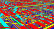
How to Panelize Your PCBs Before Lunch with Altium Designer
Whether you have a slew of PCBs to mass produce for your customers or a handful of project boards you wish to prototype all in one simple swoop, panelization is an effective way to bring high amounts of efficiency to your production.

Blog
•
May 5, 2020
Helpful Tips for Interactive Routing in Altium Designer
Before you jump into the software, you should know the types of things you’re going to want to look out for. Traces, connection lines, differential pair routing, and route paths can all affect the routing process of your board. Make sure that you’re equipped knowing, ultimately, what you want your board design to accomplish and furthermore, where you anticipate potential problem areas to be.
Blog
•
How PCB Design Engineers Can Securely Share Design Files with External Teams
Learn how PCB design engineers can securely share design files with team members, clients, and manufacturers. Marek Orzeł explores best practices and tools to protect your intellectual property while ensuring efficient collaboration.

Blog
•
OEMs and Harness Manufacturers: Building Strong Collaboration for Success
Strong partnerships between OEMs and harness manufacturers are key to efficient, high-quality product development. In this article, Krishna Sundaram shows how collaboration, clear communication, and the right design tools can streamline the harness manufacturing process and drive success.
Blog
•
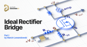
Ideal Rectifier Bridge
Read Marcin Lewandowski's article explaining how MOSFETs are replacing traditional diodes for reverse polarity protection. Step into the future of energy-efficient electronics!
Blog
•
Master Your Circuit Design: Dive into Worst Case Analysis
Dive into Worst Case Analysis techniques with Kamil Jasiński and ensure the reliability of your circuits. Master sensitivity analysis, Monte Carlo simulations, and more to confidently address real-world challenges.
Blog
•
Overview of the Gerber X3 File Format
Want to learn how the Gerber X3 file format simplifies data exchange by unifying assembly and fabrication details in a single file? This article explores the format and its role in streamlining PCB manufacturing.
Blog
•
Save Time and Prevent Errors in Cable Harness Design Today
Our new article explores best practices and tools for streamlining cable harness design workflows. Learn how to minimize errors, save time, and enhance collaboration by leveraging advanced features in Altium Designer.
Blog
•
Mastering EMI Control in PCB Design: How to Design PCBs for Low EMI
This article by Dario Fresu delves into effective techniques for designing PCBs to reduce electromagnetic interference (EMI). It covers key topics such as stackup selection, routing strategies, and grounding best practices, offering actionable insights for improved performance.

Blog
•
Altium and Renesas’ Role in Enabling Economy 4.0 is the Subject of New Documentary
Altium and Renesas are featured in a new CBS-produced documentary exploring how digitalization and cloud platforms are revolutionizing electronics production for Economy 4.0, driving efficiency and accelerating innovation.
Blog
•
Avoid Wiring Errors with Tools Tailored for Harness-to-PCB Integration
Discover how to streamline your wiring projects with advanced harness and PCB integration tools in Altium Designer. This article explores techniques to prevent wiring errors, enhance collaboration, and ensure accurate design documentation for complex projects.

Blog
•
Happy Holidays!!!
Altium wishes you all the best this holiday season! May this time be filled with joy, laughter, and cherished moments with your family and friends. We also extend our warmest wishes for a Happy New Year 2025!
Blog
•
What Is Wire Harness Design?
Explore our latest article to learn the fundamentals of wire harness design, its key components, and how it ensures organized, efficient, and reliable electrical systems across automotive, aerospace, and medical sectors.
Blog
•
How to Determine Ferrite Bead Circuit Model Parameters
Learn how to accurately determine ferrite bead circuit model parameters for effective noise suppression in high-speed PCB designs. This article explores key concepts, measurement techniques, and practical tips for modeling ferrite beads in your projects.
Blog
•
Mastering EMI Control in PCB Design: How to Choose the Stackup for EMC Design
This article by Dario Fresu, part of the Mastering EMI Control in PCB Design series, explores strategies for selecting PCB stackups to optimize EMC performance. It offers actionable tips for balancing cost, manufacturability, and signal integrity in your designs.

Blog
•
AI Vision with the Kria KV260 Vision AI Starter Kit
Discover AI-driven vision capabilities with the Kria KV260 Vision AI Starter Kit, presented by Ari Mahpour. Ideal for prototyping vision solutions, this kit offers an accessible entry point into advanced AI applications.

Blog
•
Model-Based Systems Engineering in the Era of Digital Twins: A Paradigm Shift in PCB and Electronics Design
Explore how Model-Based Systems Engineering (MBSE) integrates with digital twins to enhance design accuracy, collaboration, and lifecycle management in modern engineering projects. This approach bridges the gap between physical systems and digital models, enabling real-time simulation and optimization.
Blog
•
Wire Bonding in Altium Designer
The Wire Bonding in Altium Designer article highlights how Altium Designer 25’s wire bonding feature streamlines complex designs for advanced assemblies like 3D stacked dies and RF modules. This tool enhances efficiency and precision, catering to modern electronic design needs.
















Your search returns no results.


