News & Updates

Blog
•
Keeping Your Circuits Dry
For the home hobbyist, protecting their electrical devices usually means keeping the coffee cup or soda can away from anything that carries a large voltage. Good practice indicates that electrical devices should be housed in an enclosure to protect expensive components and reduce the risk of electric shocks from exposed circuitry. However, what do you do if the fantastic new device you’ve designed needs to work in a humid, damp, or dripping wet environment?
Blog
•
Tips for Updating Old PCB Designs with New Parts
Have you ever opened up an old design and wondered how much of it was still usable? Maybe you were contacted by an old client, and they want you to provide some updates on an old design. No matter what the situation is, there are times where updating old PCB designs with new parts makes sense. If done correctly and when armed with all the right information up front, you can cut down the total design time while preserving the best parts of your design in a new iteration. Here’s what you can do to update your old designs successfully and how your PCB design features can help.

Blog
•
How to Involve Customers in PCB Product Development
The more complex the product gets, the more involved your customer will need to be to ensure you’re designing to their requirements. When you’re using a data sharing system that integrates with your PCB design tools, it’s easy to give your customers visibility into the product development process. Altium 365 is the only system that integrates with Altium Designer® and gives you the ability to give anyone access to your PCB projects, including your customers and manufacturer.

Blog
•
Managing PCB Manufacturing Quality Control in the Cloud
Anytime you’re looking for a fabricator to produce your new design, you should ensure they have a robust quality control program. Where can quality defects arise and how can manufacturers quickly get this information back to a design team? Sometimes emails can leave too much ambiguity and it is difficult to track progress on specific design changes in the PCB layout. If you’re planning to put a new design into high volume production, there are some basic points that should be checked during fabrication and assembly as part of a PCB manufacturing quality control program.
Blog
•
Controlling Crosstalk In Connector Pinouts
Controlling crosstalk is one of the key goals in any PCB design. In most instances, when we talk about crosstalk, it’s in reference to the unwanted interaction of the electromagnetic field traveling on one transmission line with a neighboring transmission line. But crosstalk can also occur in the connector pin out. This article will describe this type of crosstalk, the types of disruptions it causes, wherein the design cycle it needs to be factored in and how it can be successfully controlled.

Blog
•
What You Can Track in Your Altium Project History
When you’re working through a new PCB design project, and you need to keep track of your project revisions, Altium 365™ creates the ideal environment for collaborative PCB design and revision tracking. Once you upload your projects onto the cloud through the Altium 365 platform, Altium 365 creates a Git repository for your project. It allows you to make it available to collaborators through Altium Designer®. This includes a complete project history, which can be easily accessed by collaborators working on a complex project.

Blog
•
Gerber Compare in Altium 365's Online Platform
The moment you push your Gerbers to a manufacturer for a DFM inspection, it can be a nerve-wracking experience waiting for a response. Before you receive your working boards, there will likely be some back-and-forth communication before your board hits the fabrication line. When manufacturers and designers need to resolve problems in Gerber files before fabrication, it helps to have a Gerber compare utility. The newest version of Altium Designer now offers this feature through the Altium 365 platform, giving everyone visibility into changes to Gerbers before fabrication.

Blog
•
California Bets on Electric Cars and Plans to Ban Gasoline Car Sales by 2035
No matter how you might feel about renewable energy and associated environmental issues, electric vehicles are becoming more mainstream and will become the primary mode of transportation in the future. For the engineering community, what’s much more interesting is how our power distribution and management infrastructure can support this shift to massive increases in the use of electricity on the grid. So what’s the rub for PCB designers?

Blog
•
My Favorite Altium Designer Keyboard Shortcuts and Viewing Features
When you’re working through a complex PCB layout, it always helps to know the shortcuts you can use to stay productive. Altium Designer® keyboard shortcuts, and keyboard + mouse shortcuts, can help you easily walk through your PCB layout during design and as part of final checks during a design review. Here are some of my favorite keyboard shortcuts and viewing options that help me stay productive, and I hope they can do the same for you.

Blog
•
The IEEE P370 Standard for High Speed PCB Interconnects
High speed PCB interconnects have continued to remain an active challenge in modeling and simulation, particularly when dealing with broadband signals. The IEEE P370 standard is a step towards addressing the challenges faced by many designers in determining broadband S-parameters for high speed structures up to 50 GHz. Although this standard has been in the works since 2015, it finally passed board approval and appears as an active draft standard.

Blog
•
Class-D Amplifier Design and PCB Layout
Amplifiers can come in all shapes and sizes, depending on their bandwidth, power consumption, and many other factors. A Class-D amplifier design is normally used with high fidelity audio systems, and circuits for a Class-D amplifier are not too difficult to build in a schematic. If you’ve never worked with a Class-D amplifier or you’re looking for a fun audio project, follow along with this PCB layout.

Blog
•
DDR5 vs. DDR6: Here's What to Expect in RAM Modules
Modern digital systems throw the digital electronics textbooks out the window, and high-speed DDR memories are a perfect example of the paradigm shift that occurs when you jump into IC and PCB design. With DDR5 still being finalized, and DDR6 now being discussed, designers who are already comfortable with DDR4 will need to consider how their design practices should adjust to accommodate the constant doubling of data speeds in these high-speed memory technologies.
Blog
•
Making the Most of Your Crystal Oscillator
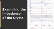
In my experience, the somewhat vague information you might find in a typical crystal datasheet doesn’t enable an engineer to be wholly confident that their design expectations can be met. On the other hand, “blindly” adopting what the crystal datasheet says usually results in adequate frequency stability. If you want to get inside and uncover what is going on, you need to start thinking about the crystal as a phase-shifting network.
Blog
•
How Antipads Affect Signal Integrity in Your Multilayer PCB
Antipads on vias and landing pads are a point of contention in modern PCB design, and the debate around the use of these elements in a multilayer PCB is framed as a binary choice. Like thermal reliefs, ground plane splits, and orthogonal routing, the debate around antipads on landing pads and vias is framed as an always/never choice. With today’s modern PCBs, it pays to understand the effects of antipads on signal integrity.
Blog
•
How to Design a Microstrip to Waveguide Transition
RF structures can be complicated to design and layout, particularly because many RF systems lead double lives as digital systems. Getting an analog signal out of a component and into a waveguide for high isolation routing is not so simple as placing a microstrip or stripline coming off your source component. Instead, you need to create a special microstrip to waveguide transition structure to ensure strong coupling into and out of your waveguide.

Blog
•
Managing PCB Polygon Pour and Copper Features in Complex Layouts
Layouts for complex electrical systems may need to make extensive use of copper pour to provide ground nets, power nets, shielding, and other copper structures for power and signal integrity. Backplanes, motherboards, RF products, and many other complex layouts will make use of copper pour and polygons that can’t be easily placed as custom components. The rules-driven design engine in Altium Designer® also ensures that any PCB polygon pour you place in your PCB layout will comply with clearance rules and will be checked against other electrical design rules.
Blog
•
High Speed Backplane Design and PCB Layout Tips
If you need to connect multiple boards into a larger system and provide interconnections between them, you’ll likely use a backplane to arrange these boards. Backplanes are advanced boards that borrow some elements from high speed design, mechanical design, high voltage/high current design, and even RF design. They carry their own set of standards that go beyond the reliability requirements in IPC.
Blog
•
PCIe 5.0 Signal Integrity and Analysis
The upcoming Gen6 version of PCIe is pushing the limits of signal integrity for many computer systems designers. As with any high-speed signaling standard, signal integrity is a major design consideration, which requires the right set of design and analysis techniques. Rather than digging deep to find PCIe 5.0 signal integrity requirements from PCI-SIG, we’ve compiled the important points for today’s PCB layout engineers. Layout engineers should pay attention here as these design requirements will become more stringent in later PCIe generations.

Blog
•
Top 4 Time Wasters in PCB Design Collaboration
An essential aspect of project management is time management, especially when your design team is working remotely. Your time management strategy is team-based and individual, but time can easily get spent on important tasks when working as part of a team. So how can you streamline important collaboration tasks for your design team to increase productivity?

Blog
•
Additive PCB Manufacturing: The Vaccine for Electronics Supply Shocks?
At this time, at least a quarter of the world’s population is under quarantine, with workers unable to go to offices or factories, leading to fundamental disabling of the world economy. The electronics industry is suffering greatly as well, dealing with a supply shock from factories shutting down in Southeast Asia, to demand-side shocks from Western markets literally shutting down. Now it is the electrical engineers taking the lead with additive PCB manufacturing.
Blog
•
Webinar "6 Steps to Master Project Storage"
Altium 365 provides a secure cloud platform to store all of your design files in a single place so you can share them with anyone and access them from anywhere. This webinar discusses the advantages of placing, storing, and working with projects in Altium 365.

Blog
•
Altium Designer 20 Changed My Layout Design Routines
I just finalized my first PCB design using Altium Designer 20. At the same time, I tested some new AD20 features, and in this article, I’ll share my thoughts about new layout design features which made the biggest impression for me: sliding, and any-angle routing.
Blog
•
Designing for Antenna Isolation in Your Wireless System
Anyone who has taken apart an old cell phone or designs IoT devices knows multiple communication capabilities are present in these designs, each requiring different antennas. The RF designer should already take precautions for interconnect isolation, but antenna isolation is just as important when modeling and designing wireless systems.

Blog
•
PCB Trace and Pad Clearance: Low vs. High Voltage
High voltage/high current designs carry safety requirements which need to be met by designers. Similarly, high speed designs need to have suppressed crosstalk in order to ensure signal integrity. The key design aspects that relate to both areas are your PCB trace clearance and pad clearance values. These design choices are critical for balancing safety, noise suppression, and manufacturability.
Blog
•
Getting Through PCB DFM
In this article, we’ll discuss the key design features to implement, and steps to take prior to fabrication that will help prevent some DFM process pain.

Blog
•
Level Up Your Design Skills - Altium Designer Getting Started User Guide Update
We are happy to announce the new update of our Altium Designer Getting Started User Guide. Whether you are new to Altium Designer or you want to brush up on some topics, the Altium Designer Getting Started User Guide will take you from a beginner to a master in PCB design.
This is only the beginning! This guide will be updated with new information based on user feedback. Let’s first go over the contents of the guide.

Blog
•
Modeling Copper Foil Roughness in Altium Designer's Impedance Profiler
With the new layer stack manager in Altium Designer®, you can now include copper foil roughness factors directly in your impedance calculator. This is quite easy to do in the layer stack manager, but it begs the question: what exactly is the copper roughness factor? Which value should be used for your interconnects?

Blog
•
High-Speed Signal Routing: The 5 Important Constraints
After you capture your schematic as an initial layout and create an initial component arrangement, it’s time to define your routing constraints. Doing this early will allow your DRC engine to spot rules violations before you finish your layout. Likewise, you’ll be able to modify the default rule set to meet your layout requirements. Here are the important routing constraints you’ll need to check before you start routing your board.
Blog
•
CoDesigner and MCAD Component Placement On-Demand Webinar
Learn how to place components from the MCAD side and synchronize them with Altium Designer ECAD models, designators, and sourcing data to simplify your design process.
Blog
•
How to Create a PCB Manufacturing Cost Estimation
Some manufacturers have very convenient PCB manufacturing cost estimation calculators you can use, but the real costs depend on a number of factors. If you’re an entrepreneur and you’re producing your own boards, or you are managing manufacturing, testing, and delivery for a new project, it’s your job to help clients understand the primary cost drivers for new boards. Here’s how you can get an estimate of your fabrication costs, both for local and overseas manufacturers.
Blog
•
PCB Mountable Connectors: SMD vs. Through-hole
Selecting a connector is as much an art as it is a science. The artistic side is all about aesthetics and satisfying clearances, while the scientific side is all about signal integrity. For PCB mountable connectors, you’ll need to choose between surface-mounted or through-hole connectors, and you’ll need to consider how each type affects signal integrity in your application. Here’s what you need to think about beyond the standard connector specifications.

Blog
•
PCB Via Current-Carrying Capacity: How Hot is Too Hot?
Trace and via current-carrying capacity are legitimate design points to focus on when designing a new board that will carry high current. The goal is to keep conductor temperatures below some appropriate limit, which then helps keep components on the board cool.
Blog
•
How to Maximize Copper in Your PCB Design: The Pros and Cons of Copper Pouring Versus Placing
There is a saying in copper pour PCB design, “Copper is free.” It means a PCB editor designer must think in reverse. A board starts off as solid copper, and the copper you don’t want is removed. It is faster to build, less consumptive, and less expensive to make a board that is mostly copper as compared to the same size board that is mostly bare. Picking the correct technique will make the difference between an effortless or frustrating experience.

Blog
•
Top 5 PCB Design Guidelines Every PCB Designer Needs to Know
What’s the key to designing a board that’s realistic on paper and in physical form? Let’s explore the top 5 design guidelines that you need to know to design your next manufacturable, functional and reliable PCB.
Blog
•
May 14, 2020
How to Highlight Nets in Altium Designer to Simplify Schematic and PCB Designs
Highlighting nets will help you simplify your schematic and PCB design. In Altium , there are multiple options that enable you to leverage this capability to simplify the verification of connections and circuit paths and make sure that the design you send to your manufacturer accurately reflects the printed circuit board you need built.










Your search returns no results.


