Welcome, Guest

Sign in to learn, create, and do more with the product you love.

News & Updates

Filters:
Tag
Blog
Eliminate Your Design Friction with Agile Teams

Design friction from scattered data and disconnected tools slows down PCB development and leads to rework. This webinar shows how Agile Teams streamlines collaboration, aligns domains, and helps teams deliver faster with fewer errors.

Embedded thumbnail for Via Dispersion: Why Propagation Delay Changes with Frequency
How-To's
Via Dispersion: Why Propagation Delay Changes with Frequency

Explore the concept of via dispersion and how it impacts propagation delay across frequencies. This tutorial walks through the math behind extracting delay from insertion loss and return loss S-parameters and explains why results can vary depending on your operating range.

Embedded thumbnail for Make Via Rule Configuration More Intuitive
New in Altium's Software
Make Via Rule Configuration More Intuitive

Set precise control over your routing via styles with new rule settings in the Physical View. Define minimum, maximum, and preferred values for both diameter and hole size, and easily switch between constraint ranges or template-based definitions for faster, more flexible design.

Blog
What is the Best Cloud PCB Design Software?

Not all cloud PCB tools are created equal, especially when design complexity increases. This article breaks down key differences between cloud-native and hybrid solutions, helping engineers choose the right approach for performance and scalability.

Blog
From Rework to Revenue: Digital PCB DFMA

This article explores how traditional, manual DFMA workflows lead to costly rework, delays, and poor collaboration across engineering teams. It shows how a connected, digital approach enables better data integrity, faster design cycles, and improved manufacturing outcomes.

Embedded thumbnail for Coplanar Ground Done Right: PCB Design Best Practices
How-To's
Coplanar Ground Done Right: PCB Design Best Practices

When is coplanar ground actually useful and when does it provide no benefit at all? If you’ve ever wondered about this, check out our brand-new video where we tackle one of the most common questions in PCB design.

Embedded thumbnail for Import and Export with Modern Mechanical Models
New in Altium's Software
Import and Export with Modern Mechanical Models

We have expanded mechanical integration by adding support for SOLIDWORKS 2024 and SOLIDWORKS 2025 part models when importing 3D bodies into the design environment. This enhancement allows designers to work with the latest mechanical models created in SOLIDWORKS without the need for additional conversions or workarounds.

Embedded thumbnail for How to Input Via Delay in Altium for DDR Routing
How-To's
How to Input Via Delay in Altium for DDR Routing

In this video, we tackle a real viewer question about DDR3 routing across multiple PCB layers and show how via delay can silently eat into your skew margin before you’ve even finished routing, using Altium’s default 10-layer stackup as a reference.

Blog
How to Choose the Right Components for Your BOM

A strong BOM can make the difference between smooth production and costly delays. Discover a practical approach to choosing components that stay available, meet compliance requirements, and keep your project on schedule.
Embedded thumbnail for Clearly Show Jumper Wires in Your Harness Designs
New in Altium's Software
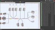
Clearly Show Jumper Wires in Your Harness Designs

Support has been improved so that jumper wires connecting two cavities within the same connector are now properly shown in Layout Drawings, making the connector wiring easier to understand during documentation and review.

Blog
From Scattered Requirements to Confident Product Development

See how the Requirements Portal transforms disconnected requirements into a single, live source of truth that engineers can trust at every stage of a project! Real customer stories in the article prove it’s already helping teams cut down on rework and bring products to market faster.


Embedded thumbnail for Why Datasheet PCB Guidelines Are Often Wrong
How-To's
Why Datasheet PCB Guidelines Are Often Wrong

Watch our brand-new video where we tackle the persistent issue of outdated PCB design guidelines still found in datasheets and application notes from major semiconductor manufacturers. Drawing on viewer comments, real-world datasheet examples, and insights from industry experts, we examine why recommendations such as splitting analog and digital ground planes (an approach rooted in the 1980s) continue to circulate despite their potential to cause EMC failures, signal integrity problems, and costly redesigns.

Blog
What is the Best PCB Design Tool For Students?

Students need PCB software that’s intuitive, affordable, and useful for building real skills. This article compares the strengths and weaknesses of leading design tools, from hobbyist platforms to industry-standard software.

Embedded thumbnail for Keep Your Harness Designs in Sync with Library Updates
New in Altium's Software
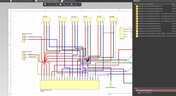
Keep Your Harness Designs in Sync with Library Updates

The "Update From Libraries" feature has been enhanced to provide broader support for harness-related objects across both Wiring Diagrams and Layout Drawings. With this expansion, a wider range of harness components such as connectors, wires, splices, and associated attributes can now be synchronized directly with their corresponding library definitions.

Blog
What Is Collaborative Engineering?

Collaborative engineering is all about breaking down silos so electrical, mechanical, and sourcing teams can work as one with shared data and real-time updates. This article shows how that approach helps you spot issues early, reduce rework, and get products out the door with fewer surprises.

Embedded thumbnail for How to Set Up Flex PCB Materials in Altium
How-To's
How to Set Up Flex PCB Materials in Altium

Discover how to set up flex and rigid-flex PCB materials in Altium with the Layer Stack Manager. In this tutorial, you’ll follow the key steps for defining polyimide cores, adhesive layers, coverlay, and stiffeners helping you build accurate, production-ready rigid-flex PCB designs.

Blog
Bend Reliability: How Trace Geometry and Materials Impact Flex Lifespan

Focused on durability under repeated mechanical stress, this piece details how routing strategy, copper thickness, adhesive systems, and bend radius selection determine flex lifespan. Engineers will find actionable recommendations for reducing strain concentration and improving long-term performance in high-cycle applications.


Embedded thumbnail for How Benchmark Unifies Hardware Development with the Altium Platform
Altium Stories
How Benchmark Unifies Hardware Development with the Altium Platform

Discover our latest customer success story and see how Benchmark streamlined hardware development using the Altium Platform. By leveraging a unified environment with real-time data, synchronized ECAD-MCAD workflows, and built-in collaboration tools, their engineering teams eliminated manual handoffs, improved cross-domain visibility, and accelerated project delivery while staying perfectly aligned.

Tag
RAM text
Blog
DDR5 vs. DDR6: Here's What to Expect in RAM Modules

Modern digital systems throw the digital electronics textbooks out the window, and high-speed DDR memories are a perfect example of the paradigm shift that occurs when you jump into IC and PCB design. With DDR5 still being finalized, and DDR6 now being discussed, designers who are already comfortable with DDR4 will need to consider how their design practices should adjust to accommodate the constant doubling of data speeds in these high-speed memory technologies.
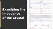
Explaining the Impedance of the Crystal
Blog
Making the Most of Your Crystal Oscillator

In my experience, the somewhat vague information you might find in a typical crystal datasheet doesn’t enable an engineer to be wholly confident that their design expectations can be met. On the other hand, “blindly” adopting what the crystal datasheet says usually results in adequate frequency stability. If you want to get inside and uncover what is going on, you need to start thinking about the crystal as a phase-shifting network.
Routed PCB
Blog
How Antipads Affect Signal Integrity in Your Multilayer PCB

Antipads on vias and landing pads are a point of contention in modern PCB design, and the debate around the use of these elements in a multilayer PCB is framed as a binary choice. Like thermal reliefs, ground plane splits, and orthogonal routing, the debate around antipads on landing pads and vias is framed as an always/never choice. With today’s modern PCBs, it pays to understand the effects of antipads on signal integrity.
PCB with RF elements
Blog
How to Design a Microstrip to Waveguide Transition

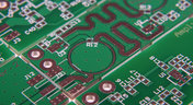
RF structures can be complicated to design and layout, particularly because many RF systems lead double lives as digital systems. Getting an analog signal out of a component and into a waveguide for high isolation routing is not so simple as placing a microstrip or stripline coming off your source component. Instead, you need to create a special microstrip to waveguide transition structure to ensure strong coupling into and out of your waveguide.

Article Preview
Blog
Managing PCB Polygon Pour and Copper Features in Complex Layouts

Layouts for complex electrical systems may need to make extensive use of copper pour to provide ground nets, power nets, shielding, and other copper structures for power and signal integrity. Backplanes, motherboards, RF products, and many other complex layouts will make use of copper pour and polygons that can’t be easily placed as custom components. The rules-driven design engine in Altium Designer® also ensures that any PCB polygon pour you place in your PCB layout will comply with clearance rules and will be checked against other electrical design rules.
Backplane printed circuit boards
Blog
High Speed Backplane Design and PCB Layout Tips

If you need to connect multiple boards into a larger system and provide interconnections between them, you’ll likely use a backplane to arrange these boards. Backplanes are advanced boards that borrow some elements from high speed design, mechanical design, high voltage/high current design, and even RF design.  They carry their own set of standards that go beyond the reliability requirements in IPC.
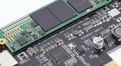
M2 Sata PCB
Blog
PCIe 5.0 Signal Integrity and Analysis

The upcoming Gen6 version of PCIe is pushing the limits of signal integrity for many computer systems designers. As with any high-speed signaling standard, signal integrity is a major design consideration, which requires the right set of design and analysis techniques. Rather than digging deep to find PCIe 5.0 signal integrity requirements from PCI-SIG, we’ve compiled the important points for today’s PCB layout engineers. Layout engineers should pay attention here as these design requirements will become more stringent in later PCIe generations.

Blog
Top 4 Time Wasters in PCB Design Collaboration

An essential aspect of project management is time management, especially when your design team is working remotely. Your time management strategy is team-based and individual, but time can easily get spent on important tasks when working as part of a team. So how can you streamline important collaboration tasks for your design team to increase productivity?

Woman work remotely
Blog
Sharing Inside and Outside Your Altium 365 Workspace

In these days of easily-available internet and quarantines, everyone is working remotely. It’s nice being able to spend time with family and regain control over your schedule, but keeping track of projects and revisions while securing user access feels like its own job. With the right set of project and data management tools, you can easily share your data with collaborators without tracking email chains.
Server storage
Blog
How Your Altium 365 Workspace Keeps You Organized

When I started using my Altium 365 Workspace for collaboration, I found I could make things run more smoothly when I kept things organized. However, I prevented any issues thanks to all the organization tools built into the Explorer panel within Altium Designer. Let’s take a look at how you can get the most value out of your Altium 365 Workspace in terms of organization and access management.
Man beside electrical schematic
Blog
How to Choose the Best PCB Manufacturer for Your Project

PCB manufacturing is competitive, and there is plenty of worldwide manufacturing capacity for new boards. If you’re looking for a manufacturer for your next project, it can be difficult to determine who is the best option to produce your board. Different fabricators and assemblers offer different levels of service, different capabilities, and access to different processes and materials. There are a lot of options to consider when selecting a manufacturer for your project.
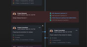
Project history in Altium Designer
Blog
Getting Started with Revision Control in Altium 365

Ever since I started using Github and Google Docs, I fell in love with revision control. Instead of keeping multiple copies of essential files and time-stamping every revision, revision tracking information gets stored alongside the file. This environment works great for code, spreadsheets, and documents, and Altium brings these same features into PCB design.

Article preview
Blog
Image Processing Embedded Systems with Modular Hardware

With advances in industrial automation, automotive technology, remote sensing, and much more, image processing is taking center stage in many embedded systems. Image processing with older video systems was difficult or impossible due to the low quality of many imaging systems with perpetual uptime. Newer systems provide video with higher frame rates and higher resolution images, but these systems still needed to connect directly to a computer in order to enable any useful image processing applications.
Article preview
Blog
Any Angle Routing: When Should You Use It?

EDA tools have come a long way since the advent of personal computing. Now advanced routing features like auto-routers, interactive routing, length tuning, and pin-swapping are helping designers stay productive, especially as device and trace densities increase. Routing is normally restricted to 45-degree or right-angle turns with typical layout and routing tools, but more advanced PCB design software allows users to route at any angle they like. So which routing style should you use, and what are the advantages of any angle routing?

Article preview
Blog
Hardware-in-the-Loop Testing: An Introduction

If you do a search for “Hardware-in-the-Loop” testing, you will frequently find examples of complex, real-time systems. Article from National Instruments, for example, gives a nice explanation and background on what hardware-in-the-loop (HIL) is, and provides an example of testing electronic control units within an automobile. In this article, we will be focusing on a smaller, more bite-sized version of HIL testing concepts.

Article preview
Blog
Near-field vs. Far-field EMI: What's Causing Noise Problems in My PCB?

If you’re an antenna designer, then you’re likely familiar with all aspects of near-field vs. far-field radiation. Given the litany of radiated EMI problems that cause noise within and outside of an electronic device, one might suddenly realize their new product is acting like a strong antenna. To understand how EMI affects your circuits, it helps to understand exactly how near-field vs. far-field radiation from your PCB affects your ability to pass EMC checks and affects your circuits.


Tag
NEW
Embedded thumbnail for Coming Soon: Advanced Via Fencing
New in Altium's Software
Coming Soon: Advanced Via Fencing

Coming soon to Altium software: Advanced Via Fencing gives you greater control over creating and managing shielding and stitching vias for RF and high-speed designs. Configure via fences directly from the Properties panel, follow traces or geometry edges, use stacked vias, define spacing and patterns, and preview the results before generating them.

NEW
Embedded thumbnail for 5 DC Power Integrity Myths That Ruin Your PCB Design
How-To's
5 DC Power Integrity Myths That Ruin Your PCB Design

DC power integrity plays a critical role in the reliability of nearly every power electronics board, yet common misconceptions can lead to costly design decisions. In this video, we break down five of the most common DC power integrity myths and explain what you really need to know for reliable power electronics design.

Embedded thumbnail for A fraction of a millimeter is the difference between a robot that fits and one that doesn't
Collaborative Engineering with Team Ribbot
A fraction of a millimeter is the difference between a robot that fits and one that doesn't

Check out the latest episode about Team Ribbot and see how they move design data between their electrical and mechanical tools without losing accuracy. Discover how Altium Designer and MCAD CoDesign help bring the boards, housings, and custom motors together right the first time with no surprises.

Embedded thumbnail for  HDI PCB Stackup Breakdown - Etching Weight Via Spacing, & More
How-To's
HDI PCB Stackup Breakdown - Etching Weight Via Spacing, & More

HDI PCB design depends on getting the stackup and manufacturing constraints right. In this deep dive, we examine a real HDI audio-interface board and explore common pitfalls, from how copper weight and etching affect minimum clearances to why solder mask slivers below 1 mil can cause manufacturing issues. You’ll also learn how proper board-edge clearance and copper pullback help protect SMD pads during routing.

Embedded thumbnail for  How do you review a robot design when your team is never in the same room?
Collaborative Engineering with Team Ribbot
How do you review a robot design when your team is never in the same room?

Team Ribbot’s engineers are spread across five states and juggle full-time jobs while building a 250-pound combat robot in their spare time. Discover how Altium Designer and Altium 365 keep the team connected, letting engineers open the live design from a laptop or phone, inspect the board in 3D, and leave comments directly on the design.

Embedded thumbnail for  Improve Visual Accuracy with True Arcs
New in Altium's Software
Improve Visual Accuracy with True Arcs

Discover how True Arc Rendering improves arc visualization in the PCB Editor and PCB Library Editor by displaying true arcs across 2D, 3D, and Board Planning modes. This provides a more accurate representation of board geometry and helps you work with curved features with greater precision throughout the design process.

Embedded thumbnail for Two engineers, one board, nobody's work gets wiped out
Collaborative Engineering with Team Ribbot
Two engineers, one board, nobody's work gets wiped out

When Team Ribbot’s electrical and mechanical engineers work on the same combat-robot design, unwanted changes can mean hours of lost work. See how Altium Designer and MCAD CoDesign let the team review and selectively accept changes, enabling seamless parallel collaboration across different locations and schedules.

Embedded thumbnail for Visualize and Refine Your Harness Designs
New in Altium's Software
Visualize and Refine Your Harness Designs

Create detailed views of bundle contents, control wire and cable paths, and rotate physical models to accurately represent the final harness assembly. These capabilities give you greater control over harness design and help ensure your digital model reflects the physical result.

Embedded thumbnail for Introducing Agentic Requirements Engineering
New in Altium's Software
Introducing Agentic Requirements Engineering

Discover a new way to work with Requirements Portal through Agentic Requirements Engineering. AI agents analyze your project data and surface proposals for your approval, reducing friction in requirements management and helping align your team's shared model with your design intent.

Embedded thumbnail for Simplify Rule Set Updates and Replacement
New in Altium's Software
Simplify Rule Set Updates and Replacement

Learn how to import rule sets with greater flexibility in Altium. When importing rules, you can add new rules to your existing set, replace only rules that match, or completely replace the current rule set giving you full control over how design rules are updated.

Embedded thumbnail for  How Team Ribbot fits 40 kW of power into a 250-pound combat robot
Collaborative Engineering with Team Ribbot
How Team Ribbot fits 40 kW of power into a 250-pound combat robot

What do you get when you pack the power of a small electric car into a combat robot with virtually no room to spare? In the first episode of our collaboration with Team Ribbot and Altium, explore how seamless ECAD-MCAD collaboration helps the team tackle complex design challenges, optimize high-performance designs, reduce errors, and bring products to life faster.

Embedded thumbnail for Just Released: Supplier Data Merging
New in Altium's Software
Just Released: Supplier Data Merging

Discover how the Supplier Data Merging feature brings together supplier information from your custom parts database and the Altium Parts Provider into a single, unified view. Access consolidated supplier data wherever supplier part numbers appear, including in ActiveBOM and during component selection.

Embedded thumbnail for How Altium’s Layer Stack Manager Actually Works
How-To's
How Altium’s Layer Stack Manager Actually Works

Take a look inside Altium's Layer Stack Manager and discover how its impedance calculator determines the ideal trace width for your target impedance. In this video, we break down the "black box" behind the calculation and show how the Simbeor-based field solver provides accurate results while eliminating the need for advanced field solver expertise.

Embedded thumbnail for Connect Requirements Directly to Your PCB Design
New in Altium's Software
Connect Requirements Directly to Your PCB Design

See how the Requirements Portal integration in Altium Designer simplifies requirements management by bringing system requirements directly into your PCB design workflow. Connect requirements to design documents, assign tasks, track verification in real time, and keep your entire team aligned with seamless synchronization in Altium 365.

Embedded thumbnail for SFP Connector Routing: High-Speed Differential Pair Design Tips
How-To's
SFP Connector Routing: High-Speed Differential Pair Design Tips

Discover practical SFP and SFP+ routing tips in our latest video, inspired by a real question from the Altium subreddit. We cover how aggressive serpentine length tuning can be, how to reduce impedance discontinuities in tight meanders, and how meandering influences mode conversion at 10G and higher data rates.

Embedded thumbnail for Handle High-Density PCB Layouts with Ease
New in Altium's Software
Handle High-Density PCB Layouts with Ease

Push the limits of PCB design with support for up to 128 signal layers, empowering the development of even the most complex, high-density boards.

Tag
Your search returns no results.