News & Updates

Blog
•
Eliminate Your Design Friction with Agile Teams
Design friction from scattered data and disconnected tools slows down PCB development and leads to rework. This webinar shows how Agile Teams streamlines collaboration, aligns domains, and helps teams deliver faster with fewer errors.


Blog
•
What Is an Integrated Design Environment for Electronics?
Using multiple disconnected tools slows down PCB development and increases the risk of errors. This article shows how an integrated environment keeps all design data connected, enabling faster workflows and fewer late-stage issues.

Blog
•
What is the Best Cloud PCB Design Software?
Not all cloud PCB tools are created equal, especially when design complexity increases. This article breaks down key differences between cloud-native and hybrid solutions, helping engineers choose the right approach for performance and scalability.

Blog
•
From Rework to Revenue: Digital PCB DFMA
This article explores how traditional, manual DFMA workflows lead to costly rework, delays, and poor collaboration across engineering teams. It shows how a connected, digital approach enables better data integrity, faster design cycles, and improved manufacturing outcomes.


Blog
•
Introducing Octopart Discover: From Part Search to Solutions Discovery
Octopart has announced Octopart Discover, a new platform that shifts electronic component search toward system-level solution discovery. The tool connects design intent with relevant options, enabling engineers to evaluate tradeoffs and identify the best-fit solutions more efficiently.


Blog
•
How to Choose the Right Components for Your BOM
A strong BOM can make the difference between smooth production and costly delays. Discover a practical approach to choosing components that stay available, meet compliance requirements, and keep your project on schedule.
Blog
•
From Scattered Requirements to Confident Product Development
See how the Requirements Portal transforms disconnected requirements into a single, live source of truth that engineers can trust at every stage of a project! Real customer stories in the article prove it’s already helping teams cut down on rework and bring products to market faster.


Blog
•
What is the Best PCB Design Tool For Students?
Students need PCB software that’s intuitive, affordable, and useful for building real skills. This article compares the strengths and weaknesses of leading design tools, from hobbyist platforms to industry-standard software.

Blog
•
What Is Collaborative Engineering?
Collaborative engineering is all about breaking down silos so electrical, mechanical, and sourcing teams can work as one with shared data and real-time updates. This article shows how that approach helps you spot issues early, reduce rework, and get products out the door with fewer surprises.

Blog
•
Bend Reliability: How Trace Geometry and Materials Impact Flex Lifespan
Focused on durability under repeated mechanical stress, this piece details how routing strategy, copper thickness, adhesive systems, and bend radius selection determine flex lifespan. Engineers will find actionable recommendations for reducing strain concentration and improving long-term performance in high-cycle applications.


Blog
•
What Makes a PCB Enclosure Rugged?
Whether you purchase products off-the-shelf or online, they all come housed within an enclosure. In some cases, these enclosures are intentionally ruggedized to withstand harsh environments or mechanical shocks. You can learn more about enclosures in this new and interesting article.
Blog
•
Concept Phase – Lid Assembly Design Part 2
We are continuing our journey through the lid assembly design phase of our Open Source Laptop project. In this section, we will discuss the layout of the test adapter and provide a demonstration of the first test for the display panel, along with the initial steps involved in assembling the boards.
Blog
•
Concept Phase – Lid Assembly Design Part 1
In the exciting next phase of the open-source laptop project we're (finally) diving into design, and getting hands-on with the display panel. Discover how we're selecting the right panel, integrating it seamlessly, and creating a custom DisplayPort adapter to illuminate the screen. Plus, learn how our choices impact features like microphones, webcams, and touch sensors, and how Altium can help bring it all to life. It’s not too late to join as we continue on this innovative journey!
Blog
•
Unleashing the Power of Concurrent PCB Design
Concurrent PCB Design is essential to unlocking the full potential of engineering teams and delivering innovative products that meet the demands of the modern world. Learn more about the main capabilities and the numerous benefits of this upcoming feature in Altium Designer.

Blog
•
Crosstalk Reduction and Elimination Techniques in Altium Designer
Whether you're designing a digital board with a ton of traces, or an RF board operating at very high frequencies, any electronic device with propagating signals will experience crosstalk. Learn more about some sure-fire ways you can reduce crosstalk in your high-speed designs.

Blog
•
Baxandall Volume Control for Audio
The Baxandall volume control is an especially useful, flexible, and simple-to-implement circuit for numerous audio designs. In this article, we will demonstrate how to design this type of equipment.

Blog
•
Common Flex Design Mistakes and How to Fix Them
Designing flexible circuits involves managing numerous factors. Discover how to prevent mistakes in this process and how to rectify them post-implementation.

Blog
•
How Much PCB Mask Expansion is Too Much?
In this article you will learn about finding the right balance between PCB mask expansion and potential problems.
Blog
•
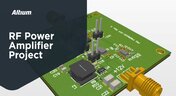
RF Power Amplifier Module PCB Design
RF power amplifiers can be found in many wireless products, often integrated into chipsets or modems. However, in certain specialized systems, you might require higher power output at a specific frequency. This necessitates a discrete amplifier circuit to deliver that power. In this article, we present an example project for a power amplifier that you can incorporate into your RF project.

Blog
•
Avoid GIGO in Your PCB Simulation Tools
Simulation tools are extremely useful for understanding electromagnetic behavior in a design. Learn more about how to avoid obtaining inaccurate results during your PCB simulation process.

Blog
•
Choosing a Converter or Regulator For Your Power Supply Design
When designing the power supply for your device, there are lots of different options. In this article, we will take a brief tour of the main choices in DC power supply design.

Blog
•
The Benefits of Ultra HDI
Learn more about the combination of using both flexible materials and ultra-HDI feature sizes in this article.

Blog
•
Understanding Power Supply Current Handling Issues: Causes and Solutions
Troubleshooting power supply current handling issues is crucial to achieving optimal performance of your electronic devices. In this article, we will explore the common reasons why a power supply fails to handle the defined output current and provide practical solutions to solving these issues.
Blog
•
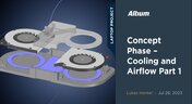
Concept Phase – Cooling and Airflow Part 1
Next step in our open-source laptop project is to explain how to design cooling and airflow. In this article, we can show you the first part of this process, such as airflow concept, fan measurement and clearance.
Blog
•
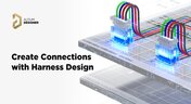
Create Connections with Harness Design
Many modern electronics have multiple boards, and connecting those different boards and systems together are harnesses. Learn more about how Altium Designer can help you create harnesses for your own multi-board designs here.

Blog
•
Do You Know How to Prevent Voltage Fluctuation?
We invite you to explore the causes of output voltage fluctuation. In this article we provide you insights on how to solve and prevent these issues.


Your search returns no results.


