News & Updates

Blog
•
Improving Supply Chain Success with BOM Management
It’s no secret that component shortages have become more frequent this year. Companies will continue to grapple with supply chain challenges into 2022 and beyond. The impact of manufacturing delays can be substantial if a part is not available. Delays occur and sales plans get put on hold. It can also be very expensive and risky to replace parts from multiple sources. Fortunately, many shortages can be avoided by introducing proactive supply chain practices.


Blog
•
Overview of PCB/PCBA Reliability and Failure Analysis
Reliability testing and failure analysis of a PCB/PCBA go hand-in-hand; when designs are stressed to the limit, their failure modes need to be determined through thorough inspection and analysis. To get started on this topic, it’s important to understand the qualification aspects that will govern your bare board design and the PCBA. We’ll look at the various dimensions of PCB/PCBA reliability, as well as some of the standard failure analysis techniques used to identify potential design change requirements.


Blog
•
When Do PCB Power Plane Resonances Occur?
By now, designers should be aware of some important behavior involved in power delivery to components in a PCB, particularly for digital components. All digital components produce and manipulate wideband signals, where the frequency content theoretically extends up to infinite frequency. As such, some radiation may propagate through your PCB, leading to resonant behavior that is not observed on the power rail.

Blog
•
How to Choose PCB Plating for Your Finished Board
Once your board passes through the standard PCB fabrication process, the bare copper in your PCB will be ready for the application of a surface finish. PCB plating is applied to protect any copper in your PCB that would be exposed through the solder mask, whether it’s a pad, via, or other conductive element. In this article, I’ll run over the different PCB plating material options and their advantages in your PCB.


Blog
•
What is the PCB Supply Chain?
The PCB supply chain encompasses multiple components, raw materials, and the PCB itself. PCBs and PCB assemblies are often the most technically complex components that are purchased for electronic assemblies and products. The complexity of modern PCBs leads to several challenges for a supply chain management team that may be significantly different when compared with other commodities the team manages. In this brief guide, we'll look in-depth at the PCB supply chain, and specifically what falls within the purview of a procurement and supply chain management team.


Blog
•
A Guide to Mode Conversion, Its Causes, and Solutions
On interconnects, such as board-to-board connections or cascaded transmission line arrangements, you have an important EMC compliance metric that is sometimes overlooked. This is mode conversion, which can be visualized in an S-parameter measurement for differential and common-mode signal transmission. In this article, we’ll look at a short overview of mode conversion in high-speed design with some examples from common differential standards.


Blog
•
PCB Via Size and Pad Size Guidelines
There are some aspects of PCB design and layout that seem deceptively simple, and yet they have a complex answer that is related to many important aspects of manufacturing. One of these design aspects is the match between PCB via size and pad size. Obviously, these two points are related; all vias have a landing pad that supports the via and provides a place to route traces into a via pad. However, there are some important sizing guidelines to follow when the matching pad and via sizes, and this match is an important element of DFM and reliability.

Blog
•
Differential Microstrip Impedance Calculator
Are you looking for a free tool that you can use to calculate the impedance of differential microstrips? We created a simple tool you can use to calculate differential microstrip impedance for a given geometry and dielectric constant. If you’ve been looking for an accurate differential microstrip impedance calculator, then the calculator below is certainly one of the best free tools you’ll find on the internet before you start using field solvers to determine differential pair impedance.


Blog
•
Getting Through a PCB DFM Check
In this article, we’ll discuss the key design features to implement, and steps to take prior to fabrication that will help prevent some common DFM problems. I’ll also provide examples of where I commonly see these PCB DFM problems in signal integrity circuits.


Blog
•
Amplifier Stability at High Frequencies and Stray Capacitance
Any time-dependent physical system with feedback and gain has conditions under which the system will reach stable behavior. Amplifier stability extends these concepts to amplifiers, where the system output can grow to an undesired saturated state due to unintended feedback. If you use the right design and simulation tools, you can easily account for potential instability in your circuit models before you create your layout.

Blog
•
Working with Design Variants
The concept of design variants entails taking a single PCB design, and then on the assembly side, modifying specific components used in the design. Either by not installing, not installing, or choosing alternate components as replacements on a specific assembly to ultimately create different end products. In that way, you could support multiple product lines. This article describes the approach to working with variants.

Blog
•
Setting Up Concord Pro Revisions and Lifecycle
Before anything else, some advice. The revisions and lifecycle are an area that takes some planning. It used to be that Concord Pro was primarily for components, but now it has gone far beyond that. With the ability to store and manage many other items, including your various templates, projects, even PDF documents, not everything will have the same revision scheme. Concord Pro is so powerful that it can handle any revision scheme you’d want to set up.

Blog
•
How to Successfully Design a BGA
Whether the board will be placed in a high pressure vessel or underwater, your design will need to withstand pressure to avoid failure. On the enclosure side, your vessel should be rated up to a certain pressure and may require frequent cycling to prevent implosion. On the electronics side, component selection and layout (especially at high voltage) become critical to preventing failure and ensuring reliability.

Blog
•
Altium Designer 20.2 Update 1 is now available
The first update of Altium Designer 20.2 and Altium NEXUS Client 3.2 is now available. You can update through the Altium Designer update system ("Extensions and Updates") or download fresh builds from the Downloads section of the Altium website. Click on "Read More" to see a list of all changes in this update.

Blog
•
How Copper Foil Roughness Affects Your Signals and Impedance
The history of engineering, both electrical and mechanical, is littered with approximations that have fallen by the wayside. These approximations worked well for a time and helped advance technology significantly over the decades. However, any model has limits on its applicability, and the typical RLCG transmission line model and frequency-independent impedance equations are no different. Copper foil roughness modeling and related transmission line impedance simulations are just one of many areas in which standard models cannot correctly treat signal behavior.

Blog
•
What is Burn-in Testing for Electronics?
Once you’re planning for production of any new board, you’ll likely be planning a battery of tests for your new product. These tests often focus on functionality and, for high speed/high frequency boards, signal/power integrity. However, you may intend for your product to operate for an extreme period of time, and you’ll need some data to reliably place a lower limit on your product’s lifetime. In addition to in-circuit tests, functional tests, and possibly mechanical tests, the components and boards themselves can benefit from burn-in testing.

Blog
•
PCB Design for Testability to Ensure High Yield and Quality
If you remember your days in school, then you probably remember the feeling of happiness and celebration when you pass a big exam. You’ll feel the same sense of adulation when your board spin passes a barrage of pre and post assembly tests, but a complex design might not reach that stage unless you implement the right design for testability methods. There are some simple steps that can help your manufacturer identify and quickly implement important bare-board and in-circuit testing (ICT), especially on critical circuit blocks.

Blog
•
Top Tips from Experienced Flex Designers
This article describes the best hints and tips for designers of rigid-flex circuits. These tips include choosing the most appropriate material, suggestions for coordinating the PCB with the manufacturer, and a set of rules to be followed while PCB design.

Blog
•
How Do Capacitor Mounting Structures And Footprints Impact Total Inductance?
There are a number of factors at play when it comes to the impact of inductance on high-frequency power distribution systems. This article will focus on the inductance of the capacitor footprint along with the inductance of vias from the capacitor footprint to the PCB power planes. Included are the various types and sizes of footprints for ceramic capacitors as well as a footprint for a tantalum capacitor; how changing the footprint impacts inductance and test results obtained for different capacitors.
Blog
•
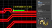
How to Perform Differential Pair Tuning in Altium Designer 20
In order to properly suppress common-mode noise, differential pairs must be routed in parallel, with perfect symmetry, and with matched lengths. In real PCBs, meeting these three objectives isn’t always possible. Instead of eyeing out your different pair lengths, the interactive routing tools in Altium Designer make differential pair length matching easy. You can encode permissible length mismatches as design rules as part of controlled impedance routing, or you can manually perform differential pair tuning using a variety of meandering styles. Here’s how this works in Altium Designer.

Blog
•
Driving Haptic Vibration and Feedback in Wearables
Augmented reality, virtual surgery, limb replacements, medical devices, and other new technologies need to incorporate haptic vibration motors and feedback to give the wearer a full sense of how they are interacting with their environment. Unless these cutting-edge applications include haptic vibration and feedback, users are forced to rely on their other four senses to understand the real or virtual environment.

Blog
•
Back Drilling Example in Altium Designer: One of the Easiest Ways to Improve Signal Integrity
Over the last 20 years, electronic devices have become increasingly sophisticated. Less than two decades ago, just having a mobile phone to make calls was rare; today, our phones power our lives. To meet the growing demand for smartphone technology, technology has become faster, more functional, and intuitive. Improvements to the component base have streamlined processes while reducing manufacturing costs.

Blog
•
Is it Simultaneous Switching Noise or Crosstalk?
Going deeper into crosstalk, there is always the issue of verifying EMI/EMC compliance through test and measurement. With the multitude of signal integrity problems that can arise in real PCBs, how can the astute designer distinguish them all? Some problems are clearer than others, with specific signal integrity measurements being developed for testing and measuring particular aspects of signal behavior. The fact is, multiple signal integrity problems could be present on a single interconnect simultaneously.

Blog
•
Sharing PCB Data with Manufacturers in the Cloud
Once you’ve finished your new project and you’re ready to push it to your manufacturer, you’ll normally be stuck in an endless email chain with an engineer, or you’ll have to share cloud links with each other. The cloud sharing and design release tools in Altium Designer and Altium Concord Pro are a huge help in this area. In this post, I’m going to take an existing project I’ve worked with in a number of recent blogs, create some fabrication and assembly documentation, and finally push this data to a manufacturer using Altium Concord Pro.

Blog
•
The Great PCB Layout "Rules of Thumb" Debate Rages On
To this day, I still see many PCB layout “rules of thumb” that first became common nearly 20 years ago. Do these rules still universally apply? The answer is a firm “maybe.” The discussion around PCB layout rules of thumb is not that these rules are correct or incorrect. The problem is that the discussion around these rules often lacks context, leading to the always/never type of discussion seen in some popular forums. My goal in this article is to communicate the context behind the common PCB design rules.
















Your search returns no results.


