News & Updates

Blog
•
Insulated Metal Substrates: Building an LED Panel
In this project we’ll be building a moderate sized LED panel on insulated metal substrate (IMS). This light panel has three different white balance High CRI LED types on it, warm, neutral and cool. By changing the brightness of the different white balances, the light from the panel can be adjusted to match other lighting, making it perfect for film use - but also creating perfect lighting for electronics work. As with all my projects, this LED panel is open source, you can find the Altium project files over on my GitHub released under the permissive MIT License.


Blog
•
DFM in PCB Material Selection
Every design should begin with selecting the materials that will appear in the PCB stackup, as well as arranging layers in the stackup to support layout and routing. This section of our PCB manufacturing andc DFM crash course focuses on selecting the right materials for your PCB design. Materials should be selected given the particular design requirements outlined in your specifications.

Blog
•
How to Start an FPGA PCB Layout For Your Embedded System
FPGAs come in quad or BGA packages that can be difficult to floorplan, especially with the high number of I/Os often implemented in these components. FPGAs offer a lot of advantages in terms of their reconfigurability, but they can require a lot of effort to layout and route without headaches. If you’ve never worked with an FPGA in your PCB layout, we have some guidelines that can help you get started.


Blog
•
How to Get 3-port S-parameters From a 2-port VNA Measurement
S-parameters are fundamental quantities in signal integrity, and an ability to understand them from measurement or analysis is very important. If you have a 3-port network, like a power divider or circulator, it may appear that you must use a 3-port VNA to measure these S-parameters. It is always acceptable to measure between two ports, but you need to know what exactly it is you are measuring. In this article, we’ll look at the relationship between the true 3-port S-parameters with a 2-port measurement.


Blog
•
A Day in the Life of the PCB Manufacturing Process
Before implementing design for manufacturing, it is important to understand the underlying process behind producing a physical PCB. Regardless of the various technologies present in each facility, a large majority of industry-leading manufacturers follow a specific set of steps to turn your design from a drawing in a CAD application into a physical board. In this article, we'll cover the basics that designers need to know as part of our crash course series on PCB manufacturing.


Blog
•
Addressing Skew Sources in High Speed PCBs
If you compile a list of skew sources, you'll see that fiber weave-induced skew is only one entry on a long list of skew sources. We'll look at this list of possible skew sources below, and we'll see how they affect the operation of your PCB. From the list below, we'll see that some of these issues with skew are not simply solved by paying attention to the fiber weave construction in a PCB substrate.

Blog
•
Should Ground Be Placed Below Inductors in Switching Regulators?
We love answering questions from our readers and YouTube viewers, and one of the recent questions we received relates to EMI from switching elements in a switching regulator is "Should a cutout be placed below the inductor in a switching regulator circuit?". Despite the variations in inductors and their magnetic behavior, there are some general principles that can be used to judge the effects of placing ground near inductors in switching regulator circuits. We’ll look at some of these principles in this article


Blog
•
Altium Designer 22.6 Update
We are happy to announce that the Altium Designer 22.6 update is now available. Altium Designer 22.6 continues to focus on improving the user experience, as well as performance and stability of the software, based on feedback from our users. Check out the key new features in the What's New section on the left side of this window!


Blog
•
Join PCB Design Review Competition from Altium
Find 9 mistakes in a PCB design and get added into the lucky draw to win a prize from Altium!


Blog
•
SAP (Semi-Additive PCB Process) – Top 5 Questions Regarding Stack Up
This Semi-Additive Process is an additional tool in the PCB fabricators' toolbox that enables them to provide feature sizes for trace width and spacing that are 25 microns, (1 mil) and below depending on the fabricators' imaging equipment. This provides much more flexibility to breakout out tight BGA areas and the ability to shrink overall circuit size and/ or reduce the number of circuit layers in the design. As the PCB design community embraces the benefits of this new printed circuit board fabrication technique, there are of course many questions to be answered.
Blog
•
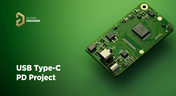
Add USB Type-C Power Delivery to Your Designs!
We want to invite you to explore the fundamentals of USB Type-C Power Delivery which is now the most popular energy transmission in current times. We will show you how to easily incorporate a dedicated PD IC into your own designs.
Blog
•
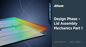
Design Phase – Lid Assembly Mechanics Part 1
It is time to delve deep into the mechanical design of our Open Source Laptop project. In this article we give you an update about the first part of fitting elements into the system. You will learn more about laptop lid, webcam integration, light sensor and microphones which will be used in this project.
Blog
•
How to Design for Test in Embedded Systems
Whether you're designing a high-speed PCB, or a complex embedded system, it will need some level of testing. In this article, we will show you some simple tricks that can make testing and debugging a prototype much easier.
Blog
•
Crosstalk Basics in PCB Design
Crosstalk is one of the most common issues related to electronics. Learn the basics of this phenomenon in PCB design, and gain knowledge on how to avoid it in your projects.
Blog
•
Top 3 Multi-Board PCB Connectivity Errors
Preparing complex PCB designs can often keep you awake at night. Learn more about some of the most common issues encountered in multi-board electrical connections.

Blog
•
Access to your Training Certificates on My Altium
Introduce an update on the My Altium user page that highlights your certificates and tracks your training progress, with one-click access to the Training Dashboard and Training Catalog pages. Easily view and share your certificates, keep an eye on your learning journey, and explore a variety of training resources.

Blog
•
Rigid-Flex PCBs: Advantages and Challenges
In this article, we will begin with a basic explanation of how rigid-flex technology differs from rigid board technology. We will then provide an overview of the advantages and conclude with a discussion of the challenges to be aware of.
Blog
•
When Should You Use Intrusive Soldering?
Through-hole components are frequently employed in power electronics, particularly when dealing with AC power from a wall outlet. In this article, you can delve into the intrusive soldering process and discover when it can be applied in PCB design.
Blog
•
Unveiling the Crucial Role of PCB Harness Design Capabilities in Multi-Board Designs
Multi-board designs are the key to meeting evolving demands, requiring robust PCB Harness Design for seamless interconnection and success. Join us as we explore the importance of PCB Harness Design capabilities and how they are crucial for the success of multi-board designs.
Blog
•
What Makes a PCB Enclosure Rugged?
Whether you purchase products off-the-shelf or online, they all come housed within an enclosure. In some cases, these enclosures are intentionally ruggedized to withstand harsh environments or mechanical shocks. You can learn more about enclosures in this new and interesting article.
Blog
•
Concept Phase – Lid Assembly Design Part 2
We are continuing our journey through the lid assembly design phase of our Open Source Laptop project. In this section, we will discuss the layout of the test adapter and provide a demonstration of the first test for the display panel, along with the initial steps involved in assembling the boards.
Blog
•
Concept Phase – Lid Assembly Design Part 1
In the exciting next phase of the open-source laptop project we're (finally) diving into design, and getting hands-on with the display panel. Discover how we're selecting the right panel, integrating it seamlessly, and creating a custom DisplayPort adapter to illuminate the screen. Plus, learn how our choices impact features like microphones, webcams, and touch sensors, and how Altium can help bring it all to life. It’s not too late to join as we continue on this innovative journey!
Blog
•
Unleashing the Power of Concurrent PCB Design
Concurrent PCB Design is essential to unlocking the full potential of engineering teams and delivering innovative products that meet the demands of the modern world. Learn more about the main capabilities and the numerous benefits of this upcoming feature in Altium Designer.
Blog
•
Crosstalk Reduction and Elimination Techniques in Altium Designer
Whether you're designing a digital board with a ton of traces, or an RF board operating at very high frequencies, any electronic device with propagating signals will experience crosstalk. Learn more about some sure-fire ways you can reduce crosstalk in your high-speed designs.

Blog
•
Baxandall Volume Control for Audio
The Baxandall volume control is an especially useful, flexible, and simple-to-implement circuit for numerous audio designs. In this article, we will demonstrate how to design this type of equipment.

Blog
•
Common Flex Design Mistakes and How to Fix Them
Designing flexible circuits involves managing numerous factors. Discover how to prevent mistakes in this process and how to rectify them post-implementation.
















Your search returns no results.


