News & Updates

Blog
•
Insulated Metal Substrates: Building an LED Panel
In this project we’ll be building a moderate sized LED panel on insulated metal substrate (IMS). This light panel has three different white balance High CRI LED types on it, warm, neutral and cool. By changing the brightness of the different white balances, the light from the panel can be adjusted to match other lighting, making it perfect for film use - but also creating perfect lighting for electronics work. As with all my projects, this LED panel is open source, you can find the Altium project files over on my GitHub released under the permissive MIT License.


Blog
•
DFM in PCB Material Selection
Every design should begin with selecting the materials that will appear in the PCB stackup, as well as arranging layers in the stackup to support layout and routing. This section of our PCB manufacturing andc DFM crash course focuses on selecting the right materials for your PCB design. Materials should be selected given the particular design requirements outlined in your specifications.

Blog
•
How to Start an FPGA PCB Layout For Your Embedded System
FPGAs come in quad or BGA packages that can be difficult to floorplan, especially with the high number of I/Os often implemented in these components. FPGAs offer a lot of advantages in terms of their reconfigurability, but they can require a lot of effort to layout and route without headaches. If you’ve never worked with an FPGA in your PCB layout, we have some guidelines that can help you get started.


Blog
•
How to Get 3-port S-parameters From a 2-port VNA Measurement
S-parameters are fundamental quantities in signal integrity, and an ability to understand them from measurement or analysis is very important. If you have a 3-port network, like a power divider or circulator, it may appear that you must use a 3-port VNA to measure these S-parameters. It is always acceptable to measure between two ports, but you need to know what exactly it is you are measuring. In this article, we’ll look at the relationship between the true 3-port S-parameters with a 2-port measurement.


Blog
•
A Day in the Life of the PCB Manufacturing Process
Before implementing design for manufacturing, it is important to understand the underlying process behind producing a physical PCB. Regardless of the various technologies present in each facility, a large majority of industry-leading manufacturers follow a specific set of steps to turn your design from a drawing in a CAD application into a physical board. In this article, we'll cover the basics that designers need to know as part of our crash course series on PCB manufacturing.


Blog
•
Addressing Skew Sources in High Speed PCBs
If you compile a list of skew sources, you'll see that fiber weave-induced skew is only one entry on a long list of skew sources. We'll look at this list of possible skew sources below, and we'll see how they affect the operation of your PCB. From the list below, we'll see that some of these issues with skew are not simply solved by paying attention to the fiber weave construction in a PCB substrate.

Blog
•
Should Ground Be Placed Below Inductors in Switching Regulators?
We love answering questions from our readers and YouTube viewers, and one of the recent questions we received relates to EMI from switching elements in a switching regulator is "Should a cutout be placed below the inductor in a switching regulator circuit?". Despite the variations in inductors and their magnetic behavior, there are some general principles that can be used to judge the effects of placing ground near inductors in switching regulator circuits. We’ll look at some of these principles in this article


Blog
•
Altium Designer 22.6 Update
We are happy to announce that the Altium Designer 22.6 update is now available. Altium Designer 22.6 continues to focus on improving the user experience, as well as performance and stability of the software, based on feedback from our users. Check out the key new features in the What's New section on the left side of this window!


Blog
•
Join PCB Design Review Competition from Altium
Find 9 mistakes in a PCB design and get added into the lucky draw to win a prize from Altium!


Blog
•
SAP (Semi-Additive PCB Process) – Top 5 Questions Regarding Stack Up
This Semi-Additive Process is an additional tool in the PCB fabricators' toolbox that enables them to provide feature sizes for trace width and spacing that are 25 microns, (1 mil) and below depending on the fabricators' imaging equipment. This provides much more flexibility to breakout out tight BGA areas and the ability to shrink overall circuit size and/ or reduce the number of circuit layers in the design. As the PCB design community embraces the benefits of this new printed circuit board fabrication technique, there are of course many questions to be answered.
Blog
•
The Ultimate Introduction to High-Speed Signal Integrity for PCB Designers
High-speed signal integrity is essential in PCB design to ensure data accuracy and system reliability. Key issues like impedance mismatches, crosstalk, and signal reflections need to be addressed through strategies such as controlled impedance traces, differential pairs, and suitable material choices. Check out our first article of the series about this topic.
Blog
•
Multi-Board PCB Signal Integrity: A Complete Guide
Our new article on signal integrity in multi-board PCBs covers essential aspects like connector pinouts, cable designs, and interconnect strategies. These factors ensure reliable performance in high-speed applications across industries such as military, aerospace, and AI.
Blog
•
Multi-CAD Support Will Be a Game Changer for Electronics Design Teams
Discover how multi-CAD support is transforming electronics design with Altium 365 by enabling seamless integration of diverse CAD file formats. This innovation addresses vendor lock-in issues, boosting collaboration, version control, and project management across different CAD tools.
Blog
•
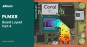
Pi.MX8 Project - Board Layout Part 4
We invite you to explore a new chapter in the PiMX8 Project, focusing on the final stages of PCB layout design for the Pi.MX8 compute module. This installment covers critical topics such as routing power planes and signal delay tuning, essential for ensuring proper functionality and performance.
Blog
•
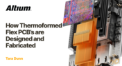
How Thermoformed Flex PCB’s are Designed and Fabricated
Thermoformed flexible PCBs are specially designed and fabricated by heating and molding them into specific shapes, making them suitable for compact and complex applications like automotive dashboards and wearable devices. This process involves precise temperature control and careful handling to ensure durability and quality. Discover more from Tara Dunn's new article.
Blog
•
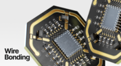
Boost Connection Integrity and Design Efficiency with Wire Bonding
Altium Designer's wire bonding feature enhances PCB design by supporting chip-up configurations for Chip on Board (CoB) designs. It offers easy validation of bond wiring in 3D views, ensuring accurate and efficient design processes. Check more about this feature on Altium's new feature page.
Blog
•
How High Frequency SMD Passives Work in a PCB Layout
High-frequency surface-mount device (SMD) passives like resistors and capacitors play a crucial role in PCB layouts, particularly in circuits operating above 1 GHz. Our article explores how these components function at high frequencies, their operational limits, and the importance of considering parasitic elements in design.

Blog
•
Essential DFM Tips for Aerospace Projects
Design for Manufacturing (DFM) is a crucial aspect of aerospace projects. This process ensures high-quality designs that meet the unique challenges of the aerospace industry, such as extreme conditions and stringent reliability standards. Learn more about essential DFM tips in our brand-new article.
Blog
•
Mechanics Meet Electronics Seamlessly in Multi-Board PCB Design
Curious about the intersection of mechanical and electrical design? Both are crucial in the PCB design process, especially for multi-board systems. Read our latest article to learn how ECAD and MCAD can address significant challenges during PCB preparation.

Blog
•
Altium 365 now has its own website!
Discover everything you need to know about Altium 365 and experience our suite of applications for secure, seamless, and streamlined collaboration. Visit now to explore how to streamline your electronic product development.
Blog
•
Efficient DC-DC Converter Design: Automated Measurements with Altium Designer 24 MixedSim
Automated measurements are no longer tough. With our Mixed Simulation mode, everything is easier. Learn more about this feature based on DC-DC buck converter design in this brand new article.
Blog
•
Altium Designer: Leading the Charge in PCB Design Innovation
In the dynamic field of electronics design, Altium Designer stands out as a pioneer, continuously advancing the boundaries of PCB (Printed Circuit Board) design. Discover the latest innovations in 3D-MID design, high-speed design, and interactive routing in this new article by David Marrakchi.
Blog
•
What Is Solder Mask Expansion and Which Value Should You Use?
Check out our new article explaining how to ensure sufficient pad area for soldering, manage misregistration tolerance, and maintain proper solder dams between components. It also highlights the role of collaboration with fabrication houses and the use of CAD tools in defining land patterns for advanced electronics designs.
Blog
•
Pi.MX8 Project - Board Layout Part 3
We continue our exploration of the Pi.MX8 open-source computer module project. In this new installment, we focus on routing planning and then cover all the layers' routing with all the details you need to know if you want to prepare a similar project.
Blog
•
Mastering Blind and Buried Vias
Check our compilation of essential resources you'll need to use blind and buried vias successfully in an HDI PCB. In our brand new article, we present the main and most valuable information about this technology, which may not be new but is still highly useful in High-Density Interconnect projects.

Blog
•
Penn Electric Racing Pushes the Envelope with Altium 365
Discover how Penn Electric Racing builds award-winning, fully electric racecars with Altium 365, pushing the boundaries of technology and design.


Your search returns no results.


