News & Updates


Blog
•
Library Importer Improvements (former Library Migrator)
Importing file-based libraries from your local computer or network drive to your Altium 365 workspace can be done using the Library Importer. Altium’s Library Migrator was renamed Library Importer—the feature’s name was changed to conform more closely to the tool’s purpose. Not only is its name new, but our team has also made several user experience improvements. We have updated the documentation to reflect this change.

Blog
•
How to Select Copper Foil for High-Frequency PCB Design
The PCB materials industry has spent significant amounts of time developing materials that provide lowest possible signal loss for products with RF applications. For high speed and high frequency designs, losses will limit signal propagation distance and distort signals, and it will create an impedance deviation that can be seen in TDR measurements. In this article, we'll look at the balance between copper foil losses and other types of losses in a PCB, as well as some strategies that are commonly used to overcome roughness.


Blog
•
Altium Designer 22.8 Update
We are happy to announce that the Altium Designer 22.8 update is now available. Altium Designer 22.8 continues to focus on improving the user experience, as well as performance and stability of the software, based on feedback from our users. Check out the key new features in the What's New section on the left side of this window!

Blog
•
What is Hybrid Beamforming?
In this article, we’ll look at beamforming implementation in an advanced method combining analog and digital techniques, known as hybrid beamforming. This method blends both digital and analog techniques to create multiple beams and thus reach multiple users with varying intensities. In the case of an RF imaging system or a radar system, hybrid beamforming in a MIMO technique also allows tracking of multiple targets with adjustable resolution.

Blog
•
Why Most Via Impedance Calculators Are Inaccurate
The problem with every via impedance calculator that I have seen is simple: they are incomplete or totally wrong. The “incomplete” part refers to a lack of context; these calculators can roughly reproduce a well-known estimate from a legend like Howard Johnson in his Digital Design textbooks. However, these calculators never provide insight into what they are actually calculating, or where the calculated via impedance is accurate. Keep reading to see why these calculators get it so wrong, as well as the context surrounding via impedance.


Blog
•
Buck Converter Simulation in Altium Designer
When designing high power circuits (usually very high voltage and/or current), you’ll need to create a regulator from scratch and place it in your PCB layout. It's also the case that you may want to model a real component using discretes in a simulation in order to qualify the system's expected operating regime. As part of buck converter design, you can easily run a buck converter simulation directly in Altium Designer’s schematic editor. Here’s how you can access these features in the newest version of Altium Designer.


Blog
•
Overview of the PCIe 6.0 Standard
Just as you get used to PCIe 5.0, they decide to release another standard! The newest iteration of PCIe is Gen6, or PCIe 6.0. PCIe 6.0 brings a doubling of channel bandwidth through introduction of PAM-4 as the signaling method in high-speed differential channels. This signaling method is a first for PCIe, and it’s an important enabler of the doubled data rate we see in the current standard. In this article, I’ll run over the important points in the standard and what PCB designers can expect when designing these channels.


Blog
•
SPI vs. I2C: How to Choose the Best Protocol for Your Memory Chips
One of the common implementations of SPI and I2C in a PCB layout is as a protocol for reading and writing to an external Flash memory. Flash chips are a very common component in embedded systems and can offer high capacities of non-volatile memory up to Gb values. When choosing a memory chip, you'll want to match the application requirements and functionality with the bus speed you need for read and write operations in your memory chip. There is also the matter of the type of Flash memory you'll need to access (NOR vs. NAND).

Blog
•
Is There an SPI Trace Impedance Requirement?
There is no SPI trace impedance requirement? The reality is that SPI lines only start to need impedance control when the length of the interconnect becomes very long. And because there is no specific impedance requirement in the bus, you have some freedom in channel design and termination. So what exactly qualifies as “very long” and when is some termination method needed? We’ll break it down in this article.


Blog
•
The Skin Effect, Current Density, and the Electromagnetic Field
During this year's AltiumLive CONNECT event, I recall receiving an interesting question about the skin effect and the distribution of current due to the presence of ground in coplanar transmission lines. In this article, we'll look at the electric field around a transmission line carrying a signal, and how this might be impacted by the skin effect.
NEW

Blog
•
What is a Multi-CAD Environment? Advantages and Best Practices
Different CAD tools shouldn't mean disconnected teams. Learn how Multi-CAD workflows help engineers review designs, collaborate across disciplines, and catch mechanical or sourcing issues before they become costly redesigns.
NEW
Blog
•
Deliver Production-Ready Multiboard PCBs Faster with Manufacturing-Driven Design
This article explores how manufacturing-driven design can help teams validate multiboard products before they reach the factory. It highlights how early checks of interconnects, harnesses, mechanical fit, sourcing, and manufacturing data can reduce late-stage changes and accelerate production readiness.

Blog
•
Stop Chasing Signatures: How Automated Design Sign-offs Accelerate Release Cycles
Automated design sign-offs can eliminate much of the administrative friction surrounding hardware approvals. This article explores how in-context reviews, structured workflows, and automated traceability help teams accelerate release cycles while maintaining control.
Blog
•
Flexible Circuits in Assembly: What PCB Designers Don’t See Until It’s Too Late
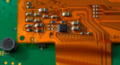
Flexible circuits introduce unique assembly challenges that aren't always visible during PCB design, from panel instability and component movement to thermal distortion during reflow. This article explains how design decisions around stiffeners, placement, panelization, and materials can improve assembly yield and reduce costly rework.

Blog
•
Requirements Management Lessons Learned: The S-80 Submarine Program
Fixing one design problem can sometimes create another you didn't see coming. This article uses the S-80 submarine program to show how better requirements traceability can help teams spot hidden impacts before they turn into expensive rework.

Blog
•
Trust Your BOM: Ensuring Design Data Integrity in Fast-Paced Hardware Projects
A BOM is only valuable if everyone can trust the data it contains. This article shows how connected BOM management helps teams eliminate errors, improve collaboration, and keep fast-moving hardware projects on schedule.
Blog
•
The Best PCB Design Rules System Keeps Your Board Error Free
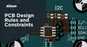
PCB design rules are the foundation of every successful layout. This article explores how defining and managing constraints helps engineers improve design accuracy, simplify verification, and deliver manufacturing-ready PCBs with confidence.

Blog
•
Why Modern Electronics Teams Are Moving to a Cloud ECAD Platform
Great products are built by connected teams, not disconnected tools. This article shows how cloud ECAD platforms enable real-time co-design, structured design reviews, and seamless collaboration across engineering, manufacturing, and supply chain teams.

Blog
•
10 Questions to Ask Your Fabricator Before Submitting a Rigid-Flex Design
A five-minute conversation with your fabricator could save weeks of redesign. Discover the ten questions that can improve manufacturability, boost yield, and help your rigid-flex project succeed on the first build.

Blog
•
Who Needs Integrated Electronic Component Search
Finding the right component shouldn't mean searching through dozens of websites and datasheets. This article shows how integrated component search helps engineers select parts faster while reducing sourcing risks and design delays.

Blog
•
How BOM Portal Supports R&D and Procurement with DFM & DFC Analysis Throughout the Entire Product Lifecycle
The best sourcing decisions happen when procurement is involved early. This webinar demonstrates how BOM Portal gives both engineering and procurement access to live lifecycle, pricing, compliance, and availability data to drive smarter decisions from prototype through production.

Blog
•
How to Design a PCB: From Schematic Capture to Manufacturing
This article walks through the complete PCB design workflow, from schematic capture and component selection to layout, design reviews, and manufacturing documentation. It highlights the key decisions at each stage that help engineering teams produce reliable, manufacturable products.
Blog
•
5 Power Integrity Myths: AC Edition
The biggest threat to your power integrity might be outdated design advice. This article challenges five common AC power integrity myths and shows what really matters when designing today's high-speed PCBs.

Blog
•
Your Design Data Has Zero Defense
Your design data may be more exposed than you think. This webinar shows how to identify common security gaps and secure engineering workflows with centralized access control and governance.

Blog
•
Flex Circuit Coverlay: Design with Lamination Processes In Mind
Your flex PCB may look perfect in CAD but coverlay doesn't stay perfectly still during manufacturing. This article reveals why designing for lamination behavior is one of the most important steps in building reliable flex circuits.

Blog
•
Integrated PCB Design vs. Legacy Point Tools: What’s the Real Cost?
As hardware development grows more collaborative, disconnected point tools can introduce data inconsistencies, traceability gaps, and costly coordination challenges. This article examines how integrated PCB design environments connect design, mechanical, supply chain, and review workflows to improve efficiency throughout the product lifecycle.













Your search returns no results.


