News & Updates
Blog
•
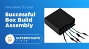
All About Box Build Assemblies
When you’re ready to manufacture a new device at production volume, there are many aspects of the product that must come together. The enclosure, cabling and connectors, embedded software/firmware, and of course the PCBA all have to be considered in totality. There is a quick way to get your product into a usable enclosure, complete with input power and cabling, and with a form factor that fits your PCBA. This overused route to a new product is a box build assembly.
Blog
•
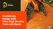
Ultra-HDI Technology is Not New
Printed circuit board fabricators have become skilled at manufacturing these technologies and also at understanding the reliability and producibility challenges associated with high-density-interconnect technology. Let’s look at where the PCB industry is at today.


Blog
•
Today's PCB Designers Are Driving Electronics Product Design
What can the industry do to support PCB designers as they continue taking a more active role in product development? Here at Altium, there has been a progressive shift towards looking at the system level and creating tools that get designers more involved throughout the product development process. As the saying goes, over the wall engineering is over… today’s most successful products are built in a collaborative process.


Blog
•
Phased Array Antenna Design for 5G Applications
As the 5G rollout progresses and researchers continue to discuss 6G, many new 5G-capable products operating in sub-GHz and mmWave bands are reaching the marketplace. Devices that will include a 5G-compatible front-end, whether small stations/repeaters or handheld devices, use phased arrays as high-gain antenna systems to provide high data throughput without losing range at higher frequencies.


Blog
•
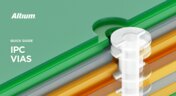
IPC - Vias
Via protection is an important part of modern PCB design. It provides additional benefits in PCB manufacturing and assembly, increasing the number of acceptable products.
Blog
•
Power Integrity Analysis in Your PCB Design Software
Power integrity problems can abound in modern PCBs, especially high-speed boards that run with fast edge rates. These systems require precise design of the PDN impedance to ensure stable power is always delivered throughout the system.



Blog
•
Schematic Compare
A design project doesn’t appear out of nowhere. The design process spreads over time, and project documents change. Schematic documents gradually become more complex, new functional blocks appear, and already finished parts can be modified and updated.

Blog
•
Embedded Capacitance Materials Overview
Capacitance is your friend whenever you need stable power integrity, which is why there is so much focus on decoupling capacitors. While these components are important and they can be used to provide targeted power integrity solutions to certain components, there is one specialty material used to supercharge capacitance in your PCB stackup or package substrate.
Blog
•
How To Import Libraries and Manage Components With Altium 365
The problems you can experience with components and libraries are endless. These problems are the most significant source of design issues and the biggest reason behind respins, costing companies untold amounts of lost profit annually.
If you want to have a better understanding of how to use Altium 365 to maintain a strong and centralized library that is free of problems and headaches, you may want to consider attending this lecture.


Blog
•
The High-Speed PCB Stackup Design Challenge
As much as we would like to build every high speed PCB perfectly, with ideal SI/PI/EMI characteristics, it isn’t always possible due to many practical constraints. Sometimes a stackup can be “good enough,” even for a high-speed PCB. This always comes from the need to balance engineering constraints, functional requirements, and the need to ensure signal and power integrity in a high-speed design, and finally to ensure compliance with EMC requirements.

Blog
•
Altium 365 now has its own website!
Discover everything you need to know about Altium 365 and experience our suite of applications for secure, seamless, and streamlined collaboration. Visit now to explore how to streamline your electronic product development.
Blog
•
Efficient DC-DC Converter Design: Automated Measurements with Altium Designer 24 MixedSim
Automated measurements are no longer tough. With our Mixed Simulation mode, everything is easier. Learn more about this feature based on DC-DC buck converter design in this brand new article.
Blog
•
Altium Designer: Leading the Charge in PCB Design Innovation
In the dynamic field of electronics design, Altium Designer stands out as a pioneer, continuously advancing the boundaries of PCB (Printed Circuit Board) design. Discover the latest innovations in 3D-MID design, high-speed design, and interactive routing in this new article by David Marrakchi.
Blog
•
What Is Solder Mask Expansion and Which Value Should You Use?
Check out our new article explaining how to ensure sufficient pad area for soldering, manage misregistration tolerance, and maintain proper solder dams between components. It also highlights the role of collaboration with fabrication houses and the use of CAD tools in defining land patterns for advanced electronics designs.
Blog
•
Pi.MX8 Project - Board Layout Part 3
We continue our exploration of the Pi.MX8 open-source computer module project. In this new installment, we focus on routing planning and then cover all the layers' routing with all the details you need to know if you want to prepare a similar project.

Blog
•
Mastering Blind and Buried Vias
Check our compilation of essential resources you'll need to use blind and buried vias successfully in an HDI PCB. In our brand new article, we present the main and most valuable information about this technology, which may not be new but is still highly useful in High-Density Interconnect projects.

Blog
•
Penn Electric Racing Pushes the Envelope with Altium 365
Discover how Penn Electric Racing builds award-winning, fully electric racecars with Altium 365, pushing the boundaries of technology and design.
Blog
•
Make Sure to Clean Your No-Clean Flux
No-clean flux has become popular due to its convenience. Learn more about why this solution is used, why cleaning might still be necessary, and how to remove no-clean flux residues. We will try to dispel all these doubts in this brand new article.

Blog
•
SPICE Simulation Module: How To Use Automated Measurements in Simulations To Save Time and Money in Design Challenges
Simulation of electronic circuits is a key factor in the success of your design. A SPICE circuit simulator may be used to speed up the design analysis. Learn more about how Altium Designer can help you with automated measurements, saving you time and money during the design process.
Blog
•
Achieve Seamless Rigid-Flex Design with Altium Designer's Unified Solution
Check out our refreshed feature page about Rigid-Flex PCB Design and see how Altium Designer’s unified environment can help you manage this kind of project with no limitations or additional licensing required.
Blog
•
How to Design a Thermal Prototype PCB
Thermal problems in PCBs often go unnoticed until prototyping, which can be costly. Design teams can't afford endless iterations, but they can conduct lower-cost thermal prototypes. Learn more about this approach in our new article.

Blog
•
6 Challenges of Managing Disconnected PLM Workflows
Discover six challenges of managing disconnected PLM workflows in electronics product development. Identify your main challenge and find the solution here.
Blog
•
DC-Aware Return Current in Mixed Signal PCBs
In this article, we will examine specific cases involving these types of components, where a very low-frequency signal or a DC signal needs to be measured, and the return path must be tracked to ensure the current loop is tight.
Blog
•
PCB Layout Replication: The Perfect Tool for Test Jigs
Replicate your circuits across multiple blocks with just a few clicks using a flawless preview pane, ensuring consistent, perfect results without the need for trial and error. Check out our new article on the PCB Layout Replication feature.
Blog
•
Durability of Pin Plating Materials for PCB Connectors
Pin headers are common components in PCBs, yet one specification often overlooked is the plating material. Discover more about plating materials for electrical connectors in our latest article.

Blog
•
4 Reasons Why We Chose AWS GovCloud (US) for Altium 365 GovCloud
In this blog, we explain the reasons behind our decision to operate Altium 365 GovCloud within AWS GovCloud (US). This partnership is guided by a clear vision: to provide our users with a secure, compliant, and reliable platform for sensitive electronics design data.







Your search returns no results.


