News & Updates

Blog
•
Altium vs KiCAD: Built to Scale From First Board to Full Product
Starting with a simple board today doesn't mean your next project will stay simple. Learn how Altium Designer and KiCAD compare when designs become more complex, teams get larger, and products move toward manufacturing.

Blog
•
Eliminate the Design-to-Production Gap with Agile Teams + Duro
Learn how Agile Teams and Duro connect design and production workflows through a unified system of record. This webinar shows how structured change management and automated data synchronization help teams reduce errors and accelerate product releases.

Blog
•
Agile Hardware Development: How to Scale Speed Without Losing Control
Agile hardware development isn’t just about working faster, it’s about working together in real time. This article explores how shared environments for ECAD, MCAD, sourcing, and requirements management eliminate handoff delays and improve decision-making across teams.

Blog
•
How Reusable Parameters in Requirements Reduce Errors and Speed Up Iterations
Verification becomes much easier when requirements and system performance data stay connected automatically. This article explains how reusable parameters and V&V rules help teams detect violations earlier and validate designs with greater confidence.


Blog
•
Complex Engineering Projects Leverage Multiple ECAD/MCAD Formats
This article explores how modern engineering teams manage complex projects involving multiple ECAD, MCAD, and manufacturing file formats across distributed workflows. It highlights the importance of design authority, disciplined revision control, and bidirectional collaboration to ensure accurate integration between PCBs and mechanical systems.
Blog
•
Avoid Costly Interconnect Errors: Essential Multiboard PCB Layout Strategies for Reliable Designs
Complex multiboard designs demand more than just connecting boards together. They require every interface to work flawlessly under real-world conditions. Discover how better pin assignments, return paths, and mechanical planning can dramatically improve reliability and reduce rework.


Blog
•
BOM Cost Optimization During Schematic Capture
Engineering and sourcing teams work best when BOM decisions happen with live market data in view. This article explains how integrated cost and availability insights help teams collaborate earlier and avoid redesigns driven by supply chain issues.
Blog
•
Why ECAD–MCAD Collaboration Is Essential to Design for Manufacturability (DFM)
Poor ECAD-MCAD coordination often leads to enclosure conflicts, connector misalignment, and costly redesigns. This article shows how integrated collaboration helps teams catch manufacturability issues earlier and keep projects moving smoothly.

Blog
•
Registration Tolerance Is Now a Design Constraint, Not a Fab Problem
Ultra HDI is changing the rules of PCB design and registration tolerance is now part of the design conversation from day one. Discover how smarter spacing, stackup planning, and collaboration with fabricators can dramatically improve manufacturability and reliability.

Blog
•
How to Use a Multicad Viewer for Seamless Collaboration
Because ECAD formats are typically incompatible, teams often struggle with versioning, conversions, and fragmented review processes. This article breaks down how multi-CAD viewers provide a unified, read-only environment that supports structured design reviews, comments, and task assignment across disciplines.


Blog
•
Best Online ECAD File Viewers for Engineers and PCB Designers
Sharing PCB designs doesn’t have to be complicated. Check out the best online ECAD viewers that let anyone view and collaborate on designs right from a browser.
Blog
•
PCB CoDesign: Design Faster Together
Experience accelerated design collaboration with PCB CoDesign, exclusively available on Altium Designer starting from December 13th. This innovative feature adopts a collaborative approach by seamlessly integrating schematic and PCB design, enabling multiple engineers to work on the same project. Explore this cutting-edge feature on our newly launched page dedicated to its functionalities.

Blog
•
6 Steps to Accelerate the Development of Complex Products
Learn the key lessons from the presentation at Iteration22; “Joe Justice, Wikispeed - Everyone Must Be a Chief Engineer at SpaceX.” Read on and discover how to speed up the development of complex products.
Blog
•
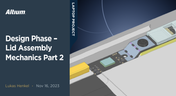
Design Phase – Lid Assembly Mechanics Part 2
We are continuing our journey into lid assembly mechanics inside the Open Source Laptop Project. In this chapter, we are focusing on the sensor PCB above the display panel.

Blog
•
How to Speed Up Your Manual Assembly Process with Assembly Assistant? The Story of XVP Photonics
Are you struggling with your manual assembly process? Would you like to speed it up and improve component placement accuracy? Read the story of XVP Photonics; with Assembly Assistant, they improved the component placement time by 25%. Discover how!

Blog
•
45V-5A Adjustable Half-Bridge DC to DC Converter
DC-to-DC buck converters are extensively employed in electronic devices. In this article, we will introduce you to one of our new projects—a DC-to-DC converter designed to serve as a power supply as well.
Blog
•
The Challenges of Modern Design: Why Requirements Management Is Essential
You need a robust requirements management process to ensure your design intent communication stays clear and organized. Read on to explore the crucial connection between well-managed requirements and today’s design.

Blog
•
Efficiency And Noise Top 10 Switching Regulator Modules
Switching regulator modules have become indispensable in a wide array of electronic devices, providing a more efficient means of voltage conversion between different levels by storing and releasing energy. Explore further insights into these devices in today's dynamic world of electronics.
Blog
•
Add USB Type-C Power Delivery to Your Designs!
We want to invite you to explore the fundamentals of USB Type-C Power Delivery which is now the most popular energy transmission in current times. We will show you how to easily incorporate a dedicated PD IC into your own designs.
Blog
•
Design Phase – Lid Assembly Mechanics Part 1
It is time to delve deep into the mechanical design of our Open Source Laptop project. In this article we give you an update about the first part of fitting elements into the system. You will learn more about laptop lid, webcam integration, light sensor and microphones which will be used in this project.

Blog
•
How to Design for Test in Embedded Systems
Whether you're designing a high-speed PCB, or a complex embedded system, it will need some level of testing. In this article, we will show you some simple tricks that can make testing and debugging a prototype much easier.
Blog
•
Crosstalk Basics in PCB Design
Crosstalk is one of the most common issues related to electronics. Learn the basics of this phenomenon in PCB design, and gain knowledge on how to avoid it in your projects.
Blog
•
Top 3 Multi-Board PCB Connectivity Errors
Preparing complex PCB designs can often keep you awake at night. Learn more about some of the most common issues encountered in multi-board electrical connections.

Blog
•
Access to your Training Certificates on My Altium
Introduce an update on the My Altium user page that highlights your certificates and tracks your training progress, with one-click access to the Training Dashboard and Training Catalog pages. Easily view and share your certificates, keep an eye on your learning journey, and explore a variety of training resources.

Blog
•
Rigid-Flex PCBs: Advantages and Challenges
In this article, we will begin with a basic explanation of how rigid-flex technology differs from rigid board technology. We will then provide an overview of the advantages and conclude with a discussion of the challenges to be aware of.
Blog
•
When Should You Use Intrusive Soldering?
Through-hole components are frequently employed in power electronics, particularly when dealing with AC power from a wall outlet. In this article, you can delve into the intrusive soldering process and discover when it can be applied in PCB design.
Blog
•
Unveiling the Crucial Role of PCB Harness Design Capabilities in Multi-Board Designs
Multi-board designs are the key to meeting evolving demands, requiring robust PCB Harness Design for seamless interconnection and success. Join us as we explore the importance of PCB Harness Design capabilities and how they are crucial for the success of multi-board designs.


Your search returns no results.


