News & Updates

Blog
•
Your Design Data Has Zero Defense
Your design data may be more exposed than you think. This webinar shows how to identify common security gaps and secure engineering workflows with centralized access control and governance.

Blog
•
Flex Circuit Coverlay: Design with Lamination Processes In Mind
Your flex PCB may look perfect in CAD but coverlay doesn't stay perfectly still during manufacturing. This article reveals why designing for lamination behavior is one of the most important steps in building reliable flex circuits.

Blog
•
Integrated PCB Design vs. Legacy Point Tools: What’s the Real Cost?
As hardware development grows more collaborative, disconnected point tools can introduce data inconsistencies, traceability gaps, and costly coordination challenges. This article examines how integrated PCB design environments connect design, mechanical, supply chain, and review workflows to improve efficiency throughout the product lifecycle.

Blog
•
Make Better Design Decisions with Signal and Power Integrity Insight
Signal integrity and power integrity are closely connected, with problems in one often affecting the other as designs become faster and more complex. This webinar explains how integrated analysis workflows help engineers evaluate PDN performance, identify potential issues early, and improve overall design quality.

Blog
•
Optimizing Your Electronics Product Design Workflow and Eliminating Bottlenecks
Every manual handoff adds time and risk to the product development process. This article shows how modern design workflows automate routine tasks, improve data visibility, and help engineering teams focus on innovation instead of administration.
Blog
•
Avoid Cross-Board Signal Integrity Issues in High-Performance Multiboard PCB Designs
Your signal may be perfect on the PCB and fail the moment it crosses a connector. This article explores the hidden SI challenges in multi-board systems and how engineers can eliminate them before they become costly debugging sessions.
Blog
•
Proto-BOM in Minutes: How BOM Portal Accelerates Component Selection
Still building BOMs the hard way? Discover how modern workflows can help you create a prototype-ready BOM faster while improving visibility into pricing, availability, and risk.
Blog
•
How to Manage Power Integrity and EMI in Complex Multiboard Systems
This article examines the challenges of maintaining power integrity and controlling EMI in complex multiboard systems. It provides practical strategies for managing return paths, connector transitions, and power distribution across interconnected assemblies.

Blog
•
Agile Teams: From Design Tool to Product Development Platform
Learn how Agile Teams evolves beyond traditional PCB design workflows to support connected product development. This webinar explores how centralized data, collaboration tools, and governance capabilities help teams accelerate delivery while maintaining control.

Blog
•
Benefits of Using an Integrated Design Environment for PCB Development
Using separate tools often creates inefficiencies and increases the risk of mistakes. This article explains how integrated design environments streamline workflows by keeping design data connected and accessible.

Blog
•
Enterprise vs. Midsize PCB Design Software: What Actually Changes at Scale
PCB design challenges change significantly as organizations scale. This article explores the key differences between mid-size and enterprise design environments, from collaboration and governance to data management and workflow automation.


Blog
•
BOM Portal vs BOM Tool: What Changes When You Upgrade
Not all BOM solutions work the same way. This article explains the key differences between BOM tools and BOM portals, and why real-time data and collaboration are becoming essential for modern electronics development.

Blog
•
Signal Mistakes Are Expensive
See how the Signal Analyzer by Keysight in Altium Designer lets you run signal integrity checks directly within your design environment. Read our article to learn how to effectively manage impedance, return paths, stackups, and more.

Blog
•
Twice the Insight. One Seamless Simulation Bundle
Ensure power and signal integrity with the Keysight Bundle in Altium Designer. Catch issues early, reduce rework, and optimize your PCBs - all within one integrated environment featuring Signal & Power Analyzer.

Blog
•
Preparing for Prototype: Final Component Validation
Final component validation is the last critical check before building a prototype, ensuring all parts are accurate, available, and viable. This article shows how Altium’s integrated tools—like SiliconExpert, Z2Data, Octopart, and BOM Portal—help teams avoid costly surprises and prepare with confidence.

Blog
•
Getting Started with Harness Design in Altium Designer 25
Explore the essential steps and tools for Harness Design in Altium Designer 25, from initial setup to final documentation. The article highlights how the unified design environment streamlines the entire process, improving efficiency and project integration.

Blog
•
The Future of PCB Design Starts Here
Altium Designer is constantly evolving, with powerful new features and updates on the way. Get an exclusive first look at what’s coming next—visit our Coming Soon page to stay up to date with the latest innovations.
Blog
•
Simplify Harness-to-System Connections for Better PCB Design Outcomes
Struggling to keep harness and system designs in sync? In our brand-new article we explore how integrating PCB and harness design workflows can eliminate errors, improve collaboration, and accelerate your development process. Discover a smarter approach to connecting your harness to the system.
Blog
•
The Crucial Balance: Cost, Quality, and Availability In Electronic Component Selection
Balancing cost, quality, and availability is key when selecting electronic components. This article explores how to make informed choices that meet design goals while managing supply chain and sourcing challenges.

Blog
•
Wire Harness Failures: The Hidden Costs and Real-World Recalls That Could Have Been Prevented
Wire harness failures can lead to significant financial losses, production delays, and safety hazards. This article delves into real-world examples of such failures across industries and illustrates how modern CAD tools can help prevent these costly issues.

Blog
•
Part Selection Fundamentals: Creating Resilient Component Requirements
Learn how to ensure electronic components meet the demands of harsh environments. This article explores key standards, testing protocols, and design considerations for building resilient systems that perform reliably under extreme conditions.
Blog
•
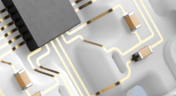
Printed Electronics: The Future of Flexible and Cost-Effective Circuit Design
This article explores the rise of printed electronics as a lightweight, flexible, and cost-effective alternative to traditional PCB design. It highlights key benefits like reduced manufacturing costs, sustainability, and new design possibilities—especially in wearables, medical devices, and automotive applications.

Blog
•
How to Choose the Best Requirements Management Tool for Electronics Development
Many electronics teams still rely on documents and spreadsheets for requirements management—leading to gaps, errors, and delays. Alexsander Tamari explores better tools to improve traceability, collaboration, and project outcomes.
Blog
•
New Routing Possibilities with Ultra HDI
Explore how Ultra HDI technology is redefining PCB design. This article breaks down the benefits and manufacturing considerations of Ultra HDI, and how it enables next-level routing density and miniaturization in advanced electronics.
Blog
•
3D-MID in Focus: Principles, Processes, and Practical Use
This article introduces 3D-MID (Mechatronic Integrated Devices), a technology that integrates circuitry into 3D plastic structures to reduce size, weight, and complexity. It explains the production process, use cases, and benefits of 3D-MID in sectors like automotive, medical, and consumer electronics.
Blog
•
Eliminate EMI and Signal Integrity Issues in Multi-Board PCB Designs
Ensure signal integrity and minimize EMI in complex electronics. Our new article explains how to address electromagnetic interference and signal integrity challenges in multi-board PCB designs, offering practical strategies and layout considerations for reliable system performance.
Blog
•
How to Overcome Power Distribution and Connector Misalignment Challenges in Multi-Board PCB Systems
Connector misalignment can compromise the reliability of power delivery in multi-board systems. This article explores the causes, effects, and prevention strategies for connector misalignment in power distribution, helping you design more robust multi-board PCB systems.
Blog
•
Mastering Component Templates in Altium Designer 25
Our new article by Dario Fresu explains how Component Templates in Altium Designer 25 Pro improve design consistency, reduce errors, and streamline collaboration. It highlights practical benefits like standardized naming, faster component creation, and scalability across projects. Includes examples of using templates with Altium 365™ to simplify complex component setup.












Your search returns no results.


