Welcome, Guest

Sign in to learn, create, and do more with the product you love.

News & Updates

Filters:
Tag
Embedded thumbnail for Dynamic Phase Matching and Tuning for Differential Pairs
New in Altium Designer 25
Dynamic Phase Matching and Tuning for Differential Pairs

Explore how dynamic phase matching for differential pairs works with the improved match length rule in Altium Designer. Learn key techniques in this quick tutorial!

Embedded thumbnail for Obey Rules and Auto-Shrinking Features
New in Altium Designer 25
Obey Rules and Auto-Shrinking Features

Discover how Altium Designer 25's Obey Rules and Auto-Shrinking features streamline routing, ensuring speed and precision while maintaining adherence to all design constraints.

Embedded thumbnail for Quickstart Guide: Single Layer PCB Design with Altium Designer 25
New in Altium Designer 25
Quickstart Guide: Single Layer PCB Design with Altium Designer 25

Transform your designs with the new Single Layer PCB Design feature in Altium Designer 25! Whether you're working on Rigid-Flex projects or creating simple, space-saving boards, this tool makes the process faster, smarter, and more efficient. Watch our guide now and unlock your next big innovation.

Blog
AI Vision with the Kria KV260 Vision AI Starter Kit

Discover AI-driven vision capabilities with the Kria KV260 Vision AI Starter Kit, presented by Ari Mahpour. Ideal for prototyping vision solutions, this kit offers an accessible entry point into advanced AI applications.


Embedded thumbnail for How to Design Bending Regions in Flex PCBs
How-To's
How to Design Bending Regions in Flex PCBs

Watch our latest video on bending regions in flex PCBs! This step-by-step guide will show you how to configure stack-ups, distinguish between flex and rigid regions, and troubleshoot common issues in 3D views.

Embedded thumbnail for LDO Regulator Essentials: From Basics to Advanced. Part V: Ripple Rejection
LDO Regulator Essentials
LDO Regulator Essentials: From Basics to Advanced. Part V: Ripple Rejection

The final part of the LDO Regulator Essentials series focuses on voltage ripple rejection in Low Dropout Regulators (LDOs). Our host Rafał Stępień explains how LDOs clean up DC supply waves, ensuring stable performance in power systems. This episode provides practical insights for optimizing sensitive designs.

Embedded thumbnail for Explore Routing Improvements in Altium Designer 25
New in Altium Designer 25
Explore Routing Improvements in Altium Designer 25

Discover Routing Improvements in Altium Designer 25. Learn about Dynamic Phase Matching, True Donut Pad Shape, and more in our latest video showcasing the powerful enhancements in our newest release.

Embedded thumbnail for Wire Bonding Shorts: Die Footprints
New in Altium Designer 25
Wire Bonding Shorts: Die Footprints

Check our new short video where Samer Aldhaher demonstrates the Wire Bonding feature in Altium Designer 25, including die-to-die and die-to-copper connections, multiple wire bonds, and pad rotation techniques.

Blog
Wire Bonding in Altium Designer

The Wire Bonding in Altium Designer article highlights how Altium Designer 25’s wire bonding feature streamlines complex designs for advanced assemblies like 3D stacked dies and RF modules. This tool enhances efficiency and precision, catering to modern electronic design needs.

Embedded thumbnail for Altium Designer 25: Collaboration at its Finest
New in Altium Designer 25
Altium Designer 25: Collaboration at its Finest

Altium Designer 25 focuses on enhancing collaboration for engineering teams with new tools like the SI Analyzer by Keysight, updated PCB CoDesign, MCAD and Ansys CoDesigners, and improved Simulation modules. This release also introduces Wire Bonding, Single Layer PCB, and performance upgrades for optimized PCB design workflows. Check our overview video about all the improvements in this release.

Embedded thumbnail for The Fastest Ways to Run a PCB BOM Review
How-To's
The Fastest Ways to Run a PCB BOM Review

Conducting a BOM review is crucial to prevent costly delays, obsolete components, and unforeseen sourcing challenges in your PCB project. Discover powerful tools like DigiKey, Octopart, and Altium 365’s BOM portal to simplify your review process and ensure you're selecting the best parts at optimal prices.

Embedded thumbnail for Quantum Systems uses Altium Designer and Altium 365 to build the future of Drones
Altium Stories
Quantum Systems uses Altium Designer and Altium 365 to build the future of Drones

Quantum Systems creates advanced drones for critical aerial intelligence across industries. With Altium Designer and Altium 365, they streamline electronics engineering and enhance team collaboration. Watch how Altium software helps them innovate faster and build reliable drones for mission-critical moments.

Embedded thumbnail for Wire Bonding Shorts: 3D Stacked Die with Cavity
New in Altium Designer 25
Wire Bonding Shorts: 3D Stacked Die with Cavity

Check our short video by Samer Aldhaher on using Altium Designer’s wire bonding tool for creating 3D stacked die in cavity. Highlights advanced techniques for compact, high-performance PCB designs with 3D integrated circuits.

Embedded thumbnail for Constraint Manager Improvements in Altium Designer 25
New in Altium Designer 25
Constraint Manager Improvements in Altium Designer 25

Discover the latest in Altium Designer 25’s Constraint Manager, with updates like flexible net selection, streamlined rule management, and differential pair handling. Simplify your PCB design workflow with powerful new tools and enhancements.

Embedded thumbnail for Signal Integrity Made Simple - Recording Preview
How-To's
Signal Integrity Made Simple - Recording Preview

Catch up on our “Signal Integrity Made Simple” webinar to explore essential techniques for ensuring high-speed design integrity. Watch the recording to gain practical insights, and don’t miss our upcoming November webinar showcasing the latest Altium Designer release, featuring the powerful Signal Analyzer by Keysight and additional tools to optimize your projects.

Tag
RF PCB
Blog
RF Power Supply Design and Layout Guide

One thing is certain: power supply designs can get much more complex than simply routing DC power lines to your components. RF power supply designs require special care to ensure they will function without transferring excessive noise between portions of the system, something that is made more difficult due to the high power levels involved. In addition to careful layout, circuitry needs to be designed such that the system provides highly efficient power conversion and delivery to each subsection of the system.
Prevent Overvoltage, Overcurrent and Heat logo
Blog
Methods to Protect your Circuit

Overvoltage, overcurrent, and heat are the three most likely events that can destroy our expensive silicon-based components or reduce our product’s life expectancy. The effects are often quite instant, but our product might survive several months of chronic overstress before giving up the ghost in some cases. Without adequate protection, our circuit can be vulnerable to damage, so what should we do? Or do we need to do anything?

SUBCKT sharing
Blog
SUBCKT Sharing: The Fastest Ways to Share SPICE Models Online

Today’s PCB designers and layout engineers often need to put on their simulation hat to learn more about the products they build. When you need to perform simulations, you need models for components, and simulation models often need to be shared with other team members at the project level or component level. What’s the best way for Altium Designer users to share this data? Read this article to learn more about sharing your models with other design participants. 
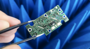
RF Printed Circuit Board
Blog
RF PCB Material Comparison for mmWave Devices

When some designers start talking materials, they probably default to FR4 laminates. The reality is there are many FR4 materials, each with relatively similar structure and a range of material property values. Designs on FR4 are quite different from those encountered at the low GHz range and mmWave frequencies. So what exactly changes at high frequencies, and what makes these materials different? To see just what makes a specific laminate useful as an RF PCB material, take a look at our guide below. 

Testing Challenges and Solutions
Blog
Low Cost Solutions for Automated Hardware in the Loop Testing

In today’s fast-paced world where iterations of electronics are spun at lightning speeds, we often forget one of the most critical aspects of development: testing. Even if we have that fancy test team, are we really able to utilize them for every modification, every small and insignificant change that we make to our prototypes? In this article, we will review a very low cost, yet highly effective and quite exhaustive test system that will get you that bang for your buck that you’ve been looking for.
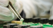
PCB Assembly
Blog
Best Practices for Using DNI/DNP Entries in Your PCB BOM

If you’ve ever looked at the BOM for a reference design or an open-source project, you may have seen a comment in some of the entries in your BOM. This comment is either “DNP” or “DNI”. If you think about it, every component placed in the PCB requires some level of placement and routing effort, which takes time and money if you’re working for a client. This begs the question, why would anyone design a board with components they don’t plan to include in the final assembly?
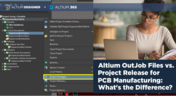
Altium Designer interface
Blog
Altium OutJob Files vs. Project Release: What's the Difference?

When it’s time to share your design data with your manufacturer, it’s like taking a leap of faith. Sending off a complete documentation package might seem as easy as placing your fab files in a zip folder, but there are better ways to ensure your manufacturer understands your project and has access to all your design data. For Altium Designer users, there are multiple options for creating and packaging release data into a complete package for your manufacturers.
Power component on PCB
Blog
Testing the Limits of Your LDO's Efficiency

If you’re designing a circuit board to be powered by anything except a bench-top regulated power supply, you’ll need to select a power regulator to place on your board. Just like any other component, your regulator has stated operating specs you’ll see in a product summary, and it has more detailed specs you’ll find in a datasheet. The fine details in your datasheets are easy to overlook, but they are the major factors that determine how your component will interact with the rest of your system.

PCB Laboratory Equipment
Blog
How Total Harmonic Distortion Affects Your Power System

It would be nice if the power that came from the wall was truly noise-free. Unfortunately, this is not the case, and although a power system can appear to output a clean sine wave, zooming into an oscilloscope trace or using an FFT will tell you a different story. When you take "dirty" power, put it through rectification, and then pass it through a switching regulator, you introduce additional noise into the system that further degrades power quality. If you’re a power supply or power systems designer, then you know the value of supplying your devices with clean, noise-free power.
Copper on PCB
Blog
What PCB Copper Thickness Should You Use?

If you’re an electronics designer or you’re just beginning your career as an engineer, the PCB stackup is probably one of the last things you’ll think about. Simple items like PCB copper thickness and board thickness can get pushed to the back burner, but you’ll need to think about these two points for many applications as not every board will be fabricated on a standard 1.57 mm two-layer PCB
Finished PCB
Blog
Should You Route Signals in Your PCB Power Plane?

I often get questions from designers asking about things like signal integrity and power integrity, and this most recent question forced me to think about some basic routing practices near planes and copper pour. "Is it okay to route signal traces on the same layer as power planes? I’ve seen some stackup guidelines that suggest this is fine, but no one provides solid advice." Once again, we have a great example of a long-standing design guideline without enough context.

PCB Routing
Blog
The Anatomy of Your Schematic Netlist, Ports, and Net Names

Electronics schematics form the foundation of your design data, and the rest of your design documents will build off of your schematic. If you’ve ever worked through a design and made changes to the schematic, then you’re probably aware of the synchronization you need to maintain with the PCB layout. At the center of it all is an important set of data about your components: your schematic netlist. What’s important for designers is to know how the netlist defines connections between different components and schematics in a large project.

Produced PCB
Blog
How to Compare PCB Manufacturing Services for Your Board

There are plenty of PCB manufacturing services you can find online, and they can all start to blend together. If you’re searching for a new service provider, it can be hard to compare all of them and find the best manufacturer that meets your needs. While experienced designers can spot bogus manufacturers from afar, there is always a temptation to go with the lowest priced, supposedly fastest overseas company you can find. However, there is a lot more that should go into choosing a PCB manufacturing service than just price.

Low-Pass Filter Arragement
Blog
Pi Filter Designs for Power Supplies

Pi Filters are a type of passive filter that gets its name from the arrangement of the three constituent components in the shape of the Greek letter Pi (π). Pi filters can be designed as either low pass or high pass filters, depending on the components used. The low-pass filter used for power supply filtering is formed from an inductor in series between the input and output with two capacitors, one across the input and the other across the output. Keep reading to learn more about their application in the PCB Design.
Hybrid PCB
Blog
How to Design a Hybrid PCB Stackup

The first question that should come up when selecting materials and planning a stackup is: what materials are needed and how many layers should be used? Assuming you’ve determined you need a low-loss laminate and you’ve determined your required layer count, it’s time to consider whether you should use a hybrid stackup. There are a few broad situations where you could consider using a hybrid stackup with low-loss laminates in your PCB

Battery and clock
Blog
Efficient Battery Power Supplies

Batteries offer a great power source for electrical devices that need to be mobile or located somewhere where connection to a mains electricity supply or other power source is impossible. The biggest problem with battery power is the expectation of users that the device will operate for significant periods with the need for recharging or replacing the batteries. This demand is placing the onus on the designer to improve efficiency and reduce power demand to meet this need.


Tag
NEW
Embedded thumbnail for Coming Soon: Advanced Via Fencing
New in Altium's Software
Coming Soon: Advanced Via Fencing

Coming soon to Altium software: Advanced Via Fencing gives you greater control over creating and managing shielding and stitching vias for RF and high-speed designs. Configure via fences directly from the Properties panel, follow traces or geometry edges, use stacked vias, define spacing and patterns, and preview the results before generating them.

NEW
Embedded thumbnail for 5 DC Power Integrity Myths That Ruin Your PCB Design
How-To's
5 DC Power Integrity Myths That Ruin Your PCB Design

DC power integrity plays a critical role in the reliability of nearly every power electronics board, yet common misconceptions can lead to costly design decisions. In this video, we break down five of the most common DC power integrity myths and explain what you really need to know for reliable power electronics design.

Embedded thumbnail for A fraction of a millimeter is the difference between a robot that fits and one that doesn't
Collaborative Engineering with Team Ribbot
A fraction of a millimeter is the difference between a robot that fits and one that doesn't

Check out the latest episode about Team Ribbot and see how they move design data between their electrical and mechanical tools without losing accuracy. Discover how Altium Designer and MCAD CoDesign help bring the boards, housings, and custom motors together right the first time with no surprises.

Embedded thumbnail for  HDI PCB Stackup Breakdown - Etching Weight Via Spacing, & More
How-To's
HDI PCB Stackup Breakdown - Etching Weight Via Spacing, & More

HDI PCB design depends on getting the stackup and manufacturing constraints right. In this deep dive, we examine a real HDI audio-interface board and explore common pitfalls, from how copper weight and etching affect minimum clearances to why solder mask slivers below 1 mil can cause manufacturing issues. You’ll also learn how proper board-edge clearance and copper pullback help protect SMD pads during routing.

Embedded thumbnail for  How do you review a robot design when your team is never in the same room?
Collaborative Engineering with Team Ribbot
How do you review a robot design when your team is never in the same room?

Team Ribbot’s engineers are spread across five states and juggle full-time jobs while building a 250-pound combat robot in their spare time. Discover how Altium Designer and Altium 365 keep the team connected, letting engineers open the live design from a laptop or phone, inspect the board in 3D, and leave comments directly on the design.

Embedded thumbnail for  Improve Visual Accuracy with True Arcs
New in Altium's Software
Improve Visual Accuracy with True Arcs

Discover how True Arc Rendering improves arc visualization in the PCB Editor and PCB Library Editor by displaying true arcs across 2D, 3D, and Board Planning modes. This provides a more accurate representation of board geometry and helps you work with curved features with greater precision throughout the design process.

Embedded thumbnail for Two engineers, one board, nobody's work gets wiped out
Collaborative Engineering with Team Ribbot
Two engineers, one board, nobody's work gets wiped out

When Team Ribbot’s electrical and mechanical engineers work on the same combat-robot design, unwanted changes can mean hours of lost work. See how Altium Designer and MCAD CoDesign let the team review and selectively accept changes, enabling seamless parallel collaboration across different locations and schedules.

Embedded thumbnail for Visualize and Refine Your Harness Designs
New in Altium's Software
Visualize and Refine Your Harness Designs

Create detailed views of bundle contents, control wire and cable paths, and rotate physical models to accurately represent the final harness assembly. These capabilities give you greater control over harness design and help ensure your digital model reflects the physical result.

Embedded thumbnail for Introducing Agentic Requirements Engineering
New in Altium's Software
Introducing Agentic Requirements Engineering

Discover a new way to work with Requirements Portal through Agentic Requirements Engineering. AI agents analyze your project data and surface proposals for your approval, reducing friction in requirements management and helping align your team's shared model with your design intent.

Embedded thumbnail for Simplify Rule Set Updates and Replacement
New in Altium's Software
Simplify Rule Set Updates and Replacement

Learn how to import rule sets with greater flexibility in Altium. When importing rules, you can add new rules to your existing set, replace only rules that match, or completely replace the current rule set giving you full control over how design rules are updated.

Embedded thumbnail for  How Team Ribbot fits 40 kW of power into a 250-pound combat robot
Collaborative Engineering with Team Ribbot
How Team Ribbot fits 40 kW of power into a 250-pound combat robot

What do you get when you pack the power of a small electric car into a combat robot with virtually no room to spare? In the first episode of our collaboration with Team Ribbot and Altium, explore how seamless ECAD-MCAD collaboration helps the team tackle complex design challenges, optimize high-performance designs, reduce errors, and bring products to life faster.

Embedded thumbnail for Just Released: Supplier Data Merging
New in Altium's Software
Just Released: Supplier Data Merging

Discover how the Supplier Data Merging feature brings together supplier information from your custom parts database and the Altium Parts Provider into a single, unified view. Access consolidated supplier data wherever supplier part numbers appear, including in ActiveBOM and during component selection.

Embedded thumbnail for How Altium’s Layer Stack Manager Actually Works
How-To's
How Altium’s Layer Stack Manager Actually Works

Take a look inside Altium's Layer Stack Manager and discover how its impedance calculator determines the ideal trace width for your target impedance. In this video, we break down the "black box" behind the calculation and show how the Simbeor-based field solver provides accurate results while eliminating the need for advanced field solver expertise.

Embedded thumbnail for Connect Requirements Directly to Your PCB Design
New in Altium's Software
Connect Requirements Directly to Your PCB Design

See how the Requirements Portal integration in Altium Designer simplifies requirements management by bringing system requirements directly into your PCB design workflow. Connect requirements to design documents, assign tasks, track verification in real time, and keep your entire team aligned with seamless synchronization in Altium 365.

Embedded thumbnail for SFP Connector Routing: High-Speed Differential Pair Design Tips
How-To's
SFP Connector Routing: High-Speed Differential Pair Design Tips

Discover practical SFP and SFP+ routing tips in our latest video, inspired by a real question from the Altium subreddit. We cover how aggressive serpentine length tuning can be, how to reduce impedance discontinuities in tight meanders, and how meandering influences mode conversion at 10G and higher data rates.

Embedded thumbnail for Handle High-Density PCB Layouts with Ease
New in Altium's Software
Handle High-Density PCB Layouts with Ease

Push the limits of PCB design with support for up to 128 signal layers, empowering the development of even the most complex, high-density boards.

Tag
Your search returns no results.