
Welcome, Guest

Sign in to learn, create, and do more with the product you love.

News & Updates

Filters:
Tag
Embedded thumbnail for Auto-tuning Your Way to Faster PCB Design
Altium Designer's 25 Quantitative Benefits
Auto-tuning Your Way to Faster PCB Design

Watch how the Auto Tuning feature in Altium Designer 25 delivers optimized DDR4 routing in a single click! Fewer steps, massive time savings. Try our Benefit Calculator to estimate your own time and cost savings.

Blog
Twice the Insight. One Seamless Simulation Bundle

Ensure power and signal integrity with the Keysight Bundle in Altium Designer. Catch issues early, reduce rework, and optimize your PCBs - all within one integrated environment featuring Signal & Power Analyzer.
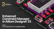

Embedded thumbnail for Enhanced Constraint Manager in Altium Designer 25. Part I: From Directives to Creepage Rules
Enhanced Constraint Manager in Altium Designer 25
Enhanced Constraint Manager in Altium Designer 25. Part I: From Directives to Creepage Rules

We are introducing a new video series on the Enhanced Constraint Manager in Altium Designer 25. In the first chapter, Samer Aldhaher demonstrates how to define net classes, apply clearance and creepage rules, and validate constraints within both the schematic and PCB. The video uses a 1kW, 400V brushless DC motor driver project to illustrate real-world applications.

Embedded thumbnail for Design Faster with Altium Designer 25
Altium Designer's 25 Quantitative Benefits
Design Faster with Altium Designer 25

Every second and every click count in the product development cycle. See how the new PCB Layout Replication feature in Altium Designer 25 boosts your efficiency in the PCB design process. Want to improve even more? Check out our Benefit Calculator now!

Embedded thumbnail for Creating PCB Drill Drawings and Tables in Altium Designer
How-To's
Creating PCB Drill Drawings and Tables in Altium Designer

If you want to learn more about drill drawings and tables in your PCB designs using Altium Designer, this tutorial is a must-watch. In the video, our Tech Consultant Zach Peterson walks you through multiple methods for generating these critical fabrication documents, including automatic Gerber outputs and custom drawings.

Embedded thumbnail for Streamlining Team Collaboration in Industrial PCB Projects - Recording Preview
New in Altium Designer 25
Streamlining Team Collaboration in Industrial PCB Projects - Recording Preview

This webinar recording shows how Altium Designer and Altium 365 improve team collaboration in industrial PCB projects. It covers features like version control, live commenting, task tracking, and JIRA integration to help teams work more efficiently and reduce costly errors.

Blog
Preparing for Prototype: Final Component Validation

Final component validation is the last critical check before building a prototype, ensuring all parts are accurate, available, and viable. This article shows how Altium’s integrated tools—like SiliconExpert, Z2Data, Octopart, and BOM Portal—help teams avoid costly surprises and prepare with confidence.

Blog
Getting Started with Harness Design in Altium Designer 25

Explore the essential steps and tools for Harness Design in Altium Designer 25, from initial setup to final documentation. The article highlights how the unified design environment streamlines the entire process, improving efficiency and project integration.

Blog
The Future of PCB Design Starts Here

Altium Designer is constantly evolving, with powerful new features and updates on the way. Get an exclusive first look at what’s coming next—visit our Coming Soon page to stay up to date with the latest innovations.
Blog
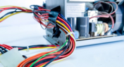
Simplify Harness-to-System Connections for Better PCB Design Outcomes

Struggling to keep harness and system designs in sync? In our brand-new article we explore how integrating PCB and harness design workflows can eliminate errors, improve collaboration, and accelerate your development process. Discover a smarter approach to connecting your harness to the system.
Embedded thumbnail for AC Coupling Capacitors: Placement for High-Speed PCB Design
How-To's
AC Coupling Capacitors: Placement for High-Speed PCB Design

Learn the facts about AC coupling capacitor placement in high-speed PCB designs. In this video, Zach Peterson explores the ongoing debate: should AC coupling capacitors be placed near the transmitter or the receiver in high-speed differential pairs?

Embedded thumbnail for Coming Soon: Export 3D-MID Tracks as Centerline Curves
New in Altium Designer 25
Coming Soon: Export 3D-MID Tracks as Centerline Curves

Coming Soon: 3D-MID Track-to-Centerline Export allows you to export conductive tracks on 3D substrates as precise centerline curves within STEP files—enabling seamless integration with advanced 5-axis manufacturing processes. Explore more upcoming upgrades on our Coming Soon page.

Embedded thumbnail for Advanced xSignal and Impedance Control Techniques - Recording Preview
New in Altium Designer 25
Advanced xSignal and Impedance Control Techniques - Recording Preview

This webinar recording explores advanced xSignal and impedance control techniques in Altium Designer 25. It covers defining xSignals, managing impedance profiles, differential pairs, and delay tuning—all essential for high-speed PCB design. Full recording you find here: April 2025 COM Webinar Recording.

Embedded thumbnail for Coming Soon: Embedded 3D Models for Harness Designs
How-To's
Coming Soon: Embedded 3D Models for Harness Designs

Coming soon: the Embedded 3D Models for Harness Designs feature will automatically include Parasolid-format 3D models in your harness layout drawings. This improves integration with MCAD CoDesigner, enabling seamless synchronization between electrical and mechanical design domains. To see more upcoming upgrades, visit our Coming Soon page.

Embedded thumbnail for Make Smarter Design Decisions with Signal Analyzer by Keysight
New in Altium Designer 25
Make Smarter Design Decisions with Signal Analyzer by Keysight

Discover how to simplify your workflow and boost design confidence with Signal Analyzer by Keysight—a complete extension available right inside Altium Designer 25. This whitepaper shows you how to analyze impedance, delay, and insertion/return loss without ever leaving your design environment.

Blog
Printed Electronics: The Future of Flexible and Cost-Effective Circuit Design

This article explores the rise of printed electronics as a lightweight, flexible, and cost-effective alternative to traditional PCB design. It highlights key benefits like reduced manufacturing costs, sustainability, and new design possibilities—especially in wearables, medical devices, and automotive applications. 

Embedded thumbnail for Unveiling 86% Task Time Efficiency in Altium Designer 25
Altium Designer's 25 Quantitative Benefits
Unveiling 86% Task Time Efficiency in Altium Designer 25

Watch how Altium Designer 25 saves time on PCB visualization. This short video shows a side-by-side comparison of the same task done in Altium Designer 25 vs. an external CAD tool—revealing big time and click savings. A great teaser to highlight the value of the unified design environment and promote the Benefit Calculator.

Tag
PCB Design Basics for New Designers
Blog
PCB Design Basics for New Designers

In this article, I’ll present some design basics that every new designer should follow to help ensure their design process is successful. Some of these points may challenge the conventional view of how circuit boards are constructed, but they are intended to help balance low noise signaling, manufacturability, and ease of solving a layout.

Selecting Materials for High Voltage PCB Design and Layout
Blog
Selecting Materials for High Voltage PCB Design and Layout

High voltage PCBs are subject to certain safety and reliability concerns that you won’t find in most other boards. If your fabrication house specializes in high voltage PCBs and keeps materials in stock, they can likely recommend a material set, as well as a standard stackup you might use for certain voltage ranges and frequencies. If you need to choose your own materials, follow the tips below to help you narrow down to the right material set.
Via tenting in PCB Layout
Blog
When to Use Tented Vias in Your PCB Layout

There are some guidelines I see many designers implement as a standard practice, often without thinking about it. Some of these practices are misunderstood or implemented without best practices. Others are implemented without thinking about the potential problems. One of these is the use of tented vias, which is sometimes implemented in a PCB layout by default. Is this always the right practice?
Capacitive load termination
Blog
How to Impedance Match and Terminate Capacitive Loads

The idea of a purely capacitive load is something of a fallacy. Yes, capacitors exist, but all capacitors are non-ideal, and it is this deviation from a theoretical capacitance that determines how to impedance match a load that exhibits capacitive behavior. Let’s take a look at this important aspect of interconnect design and see what it really means to terminate a capacitive load.
Using Altium 365 Over Your Vanilla Version Control System
Blog
Using Altium 365 Over Your Vanilla Version Control System

There are all sorts of version control systems out there that people have been using with their PCB design software. As discussed in Why Use a Version Control System, we looked at different options ranging for local hard drive storage to sophisticated online revisioning systems. In this article we will be reviewing the differences between a standard VCS and Altium 365.
Why Use a Version Control System in PCB Design
Blog
Why Use a Version Control System in PCB Design

Version Control Systems (VCS) have been around for many decades within the software world but can be surprisingly new to some folks in the electronics design industry. This article will cover what a VCS is, what it does, and why you should be using one for your PCB design projects.

IPC 6012 Class 3 Annular Ring
Blog
Meeting Standards: IPC 6012 Class 3 Annular Ring

Designers often conflate leftover annular ring and pad sizes - they need to place a sufficiently large pad size on the surface layer to ensure that the annular ring that is leftover during fabrication will be large enough. As long as the annular ring is sufficiently large, the drill hit will not be considered defective and the board will have passed inspection. In this article, I'll discuss the limits on IPC-6012 Class 3 annular rings as these are a standard fabrication requirement for high-reliability rigid PCBs.
PCB fabrication notes
Blog
Decoding PCB Fabrication Notes

Sending a board out for fabrication is an exciting and nerve-wracking moment. Why not just give your fabricator your design files and let them figure it out? There are a few reasons for this, but it means the responsibility comes back to you as the designer to produce manufacturing files and documentation for your PCB. It’s actually quite simple if you have the right design tools. We’ll look at how you can do this inside your PCB layout and how this will help you quickly generate data for your manufacturer.

HDI PCB design and HDI PCB manufacturing process
Blog
Design Basics for HDI and the HDI PCB Manufacturing Process

As the world of technology has evolved, so has the need to pack more capabilities into smaller packages. PCBs designed using high-density interconnect techniques tend to be smaller as more components are packed in a smaller space. An HDI PCB uses blind, buried, and micro vias, vias in pads, and very thin traces to pack more components into a smaller area. We’ll show you the design basics for HDI and how Altium Designer® can help you create a powerful HDI PCB.
All About PCB Test Points
Blog
Is It Printed or a Component? All About PCB Test Points

Test points in your electronic assembly will give you a location to access components and take important measurements to verify functionality. If you’ve never used a test point or you’re not sure if you need test points, keep reading to see what options you have for test point usage in your PCB layout.

How to Design to a Differential Impedance Specification
Blog
How to Design to a Differential Impedance Specification

The concept and implementation of differential impedance are both sometimes misunderstood. In addition, the design of a channel to reach a specific differential impedance is often done in a haphazard way. The very concept of differential impedance is something of a mathematical construct that doesn’t fully capture the behavior of each signal in a differential trace. Keep reading to see a bit more depth on how to design to a differential impedance spec and exactly what it means for your design.
Product Lifecycle Management in Electronics Manufacturing
Blog
Product Lifecycle Management in Electronics Manufacturing

An effective product lifecycle management (PLM) solution will integrate the tools and processes employed to design, develop and manufacture a new device. This solution goes beyond engineering activities to include the project management, process control, and financial management of the end-to-end business processes. PLM solutions create this collaborative environment where product development can flourish, bringing additional benefits in efficiencies and transparent communications, breaking silos, and speeding up the development process.
Tight versus loose coupling
Blog
Should You Use Tight vs. Loose Differential Pair Spacing and Coupling?

In this article, we want to get closer to a realistic description of tight coupling vs. loose coupling in terms of differential pair spacing, as well as how the differential pair spacing affects things like impedance, differential-mode noise, reception of common-mode noise, and termination. As we’ll see, the focus on tight coupling has its merits, but it’s often cited as necessary for the wrong reasons.

Engineering Design Review Guide
Blog
How to Solve Your Engineering Design Review Challenges

You’ve possibly gone through plenty of engineering design reviews, both on the front-end of a project and the back-end before manufacturing. Engineering design reviews are performed to accomplish multiple objectives, and with many engineering teams taking a systems-based approach to design and production, electronics design teams will need to review much more than just a PCB layout and BOM. Today’s challenges with sourcing, manufacturability, reliability, and mechanical constraints are all areas that must be confronted in real designs
Schematic Review Checklist
Blog
Schematic Review Checklist

One of the most common points of failure of a device occurs even before you start to layout your circuit board. Mistakes in your schematic design can easily make their way all the way into prototypes or production without a second thought once layout starts. In this article, I’m not going to extol the virtues of a good schematic design. Instead, this article is a simple no frills checklist.

Tag
Embedded thumbnail for Skip Layer Routing for RF: Control Impedance & Cut Insertion Loss
How-To's
Skip Layer Routing for RF: Control Impedance & Cut Insertion Loss

Discover our latest video and learn how RF designers use a deeper ground plane to minimize skin-effect resistance, improve signal integrity over long high-frequency routes, and optimize impedance matching for oversized SMT pads in antenna launches and coaxial connectors.

Embedded thumbnail for Just Released: ODB++ Intellectual Property Protection
New in Altium's Software
Just Released: ODB++ Intellectual Property Protection

ODB++ Intellectual Property Protection lets you control exactly what design data is included in the ODB++ output, ensuring each manufacturing partner receives only the information needed for their specific fabrication or assembly tasks.

Embedded thumbnail for Future of Electronics Development in Security and Aerospace
How-To's
Future of Electronics Development in Security and Aerospace

See the highlights from Altium's executive event in Hamburg, where Security and Aerospace leaders explored AI-driven development, digital engineering, supply chain resilience, and the future of mission-critical electronics.

Embedded thumbnail for Create Clearance Rules Faster and with Less Effort
New in Altium's Software
Create Clearance Rules Faster and with Less Effort

Setting up clearance rules is now more intuitive in the Constraint Manager. Choose the Simple view for faster configuration with grouped object types, or the Advanced view when you need detailed, matrix-based clearance control.

Embedded thumbnail for Mastering HDI Design Rules in Altium Designer
How-To's
Mastering HDI Design Rules in Altium Designer

In our latest Altium Academy tutorial, we guide you through configuring the essential HDI PCB design rules in Altium's software. You'll learn how to use your manufacturer's fabrication capabilities to create accurate design rules and constraints for your PCB.

Embedded thumbnail for Search, Filter, and Navigate PCB Designs Faster
New in Altium's Software
Search, Filter, and Navigate PCB Designs Faster

The Web Viewer now features a redesigned search experience for faster access to PCB design data across supported CAD formats. A lightweight, intuitive interface lets you begin with simple search terms and progressively refine results using contextual suggestions.

Embedded thumbnail for Gain Better Control Over Wire Bond Visibility
New in Altium's Software
Gain Better Control Over Wire Bond Visibility

New bond wire visibility controls give you greater flexibility when working with wire-bonded boards and footprints, making it easier to focus on the details that matter most.

Embedded thumbnail for Coming Soon: Selectable Harness Source Within Multi-board Design
New in Altium's Software
Coming Soon: Selectable Harness Source Within Multi-board Design

Selectable Harness Source Within Multi-board Design enables harness projects to drive system connectivity while maintaining bidirectional synchronization between multi-board schematics and harness wiring diagrams for improved accuracy and easier design management.

Embedded thumbnail for Choose the Simbeor Version for Your PCB Calculations
New in Altium's Software
Choose the Simbeor Version for Your PCB Calculations

The PCB Editor now lets you choose the Simbeor version used for delay and impedance calculations, giving you more flexibility and consistency across your design workflows.

Embedded thumbnail for Improve PCB Editor Performance with Via Instancing
New in Altium's Software
Improve PCB Editor Performance with Via Instancing

The PCB Editor now uses via instancing to generate geometry for each via individually, providing greater flexibility and a more advanced approach to managing vias in PCB designs.

Embedded thumbnail for GSSG Stackup Deep Dive: Routing, Impedance, and HDI
How-To's
GSSG Stackup Deep Dive: Routing, Impedance, and HDI

A ground-signal-signal-ground (GSSG) stackup rethinks the traditional four-layer PCB structure by moving the ground planes to the outer layers and routing signals on the two inner layers. In this Altium Academy deep dive, we review a real one-minute design review submission and demonstrate how to configure a GSSG stackup properly using the Layer Stack Manager.

Embedded thumbnail for Generate IPC-7351B Compliant Footprints with More Control
New in Altium's Software
Generate IPC-7351B Compliant Footprints with More Control

The IPC Compliant Footprint Wizard has been updated to improve IPC-7351B compliance across supported package types. Enhancements include footprint calculations, package outlines, silkscreen and courtyard generation, layer mapping, density table behavior, and new pad trimming controls for gullwing packages, with support added to the batch generator Excel template.

Embedded thumbnail for Add Unit-Aware Temperature Coefficient Parameters
New in Altium's Software
Add Unit-Aware Temperature Coefficient Parameters

Component templates in a connected Workspace on the Altium Platform now include support for Temperature Coefficient (ppm/°C) as a unit-aware user parameter type. This makes it possible to define temperature coefficient values directly within the template using the appropriate units.

Embedded thumbnail for When to Add Part Numbers to SMD Passives
How-To's
When to Add Part Numbers to SMD Passives

Check out our new video covering essential electronics fundamentals, with a focus on why including part numbers for SMD passive components, such as SMD resistors, directly on schematics is so important. We also explore whether relying only on the Bill of Materials (BOM) is enough for effective electronic component management.

Embedded thumbnail for Present Large Harness Tables More Clearly
New in Altium's Software
Present Large Harness Tables More Clearly

Harness Draftsman now supports splitting connection tables across multiple pages in *.HarDwf documents. With the new page height limit setting, you can easily control how much of the table appears on each page.

Embedded thumbnail for Innovate Beyond - The Future of Electronics Development in Automotive
How-To's
Innovate Beyond - The Future of Electronics Development in Automotive

Discover how the future of automotive electronics is being shaped by a more connected development approach that unifies teams, data, requirements, design, collaboration, and manufacturing. Recorded at BMW Welt and the BMW Museum during Altium’s "The Future of Electronics Development in Automotive" event, this video explores the key challenges and innovations driving the next generation of automotive design.

Tag
Your search returns no results.