News & Updates
Blog
•
Flexible Circuits in Assembly: What PCB Designers Don’t See Until It’s Too Late
Flexible circuits introduce unique assembly challenges that aren't always visible during PCB design, from panel instability and component movement to thermal distortion during reflow. This article explains how design decisions around stiffeners, placement, panelization, and materials can improve assembly yield and reduce costly rework.


Blog
•
Requirements Management Lessons Learned: The S-80 Submarine Program
Fixing one design problem can sometimes create another you didn't see coming. This article uses the S-80 submarine program to show how better requirements traceability can help teams spot hidden impacts before they turn into expensive rework.

Blog
•
Trust Your BOM: Ensuring Design Data Integrity in Fast-Paced Hardware Projects
A BOM is only valuable if everyone can trust the data it contains. This article shows how connected BOM management helps teams eliminate errors, improve collaboration, and keep fast-moving hardware projects on schedule.

Blog
•
The Best PCB Design Rules System Keeps Your Board Error Free
PCB design rules are the foundation of every successful layout. This article explores how defining and managing constraints helps engineers improve design accuracy, simplify verification, and deliver manufacturing-ready PCBs with confidence.


Blog
•
Why Modern Electronics Teams Are Moving to a Cloud ECAD Platform
Great products are built by connected teams, not disconnected tools. This article shows how cloud ECAD platforms enable real-time co-design, structured design reviews, and seamless collaboration across engineering, manufacturing, and supply chain teams.


Blog
•
10 Questions to Ask Your Fabricator Before Submitting a Rigid-Flex Design
A five-minute conversation with your fabricator could save weeks of redesign. Discover the ten questions that can improve manufacturability, boost yield, and help your rigid-flex project succeed on the first build.

Blog
•
Who Needs Integrated Electronic Component Search
Finding the right component shouldn't mean searching through dozens of websites and datasheets. This article shows how integrated component search helps engineers select parts faster while reducing sourcing risks and design delays.


Blog
•
How BOM Portal Supports R&D and Procurement with DFM & DFC Analysis Throughout the Entire Product Lifecycle
The best sourcing decisions happen when procurement is involved early. This webinar demonstrates how BOM Portal gives both engineering and procurement access to live lifecycle, pricing, compliance, and availability data to drive smarter decisions from prototype through production.

Blog
•
How to Design a PCB: From Schematic Capture to Manufacturing
This article walks through the complete PCB design workflow, from schematic capture and component selection to layout, design reviews, and manufacturing documentation. It highlights the key decisions at each stage that help engineering teams produce reliable, manufacturable products.

Blog
•
5 Power Integrity Myths: AC Edition
The biggest threat to your power integrity might be outdated design advice. This article challenges five common AC power integrity myths and shows what really matters when designing today's high-speed PCBs.

Blog
•
Wire Harness Design Guide for Development and Manufacturing
Designing a wire harness goes far beyond just connecting components—it’s about ensuring manufacturability, reliability, and compliance. This article walks you through the entire process, from initial design to production, helping you streamline development and avoid common pitfalls.

Blog
•
Preparing for Medical Device Cybersecurity Assessments
Explore the key considerations and best practices for conducting cybersecurity assessments in medical device development. This article outlines how to identify potential threats, evaluate risks, and ensure compliance with evolving industry standards.
Blog
•
Harness Complexity, Design with Simplicity
Harness Design in Altium Designer simplifies managing PCB interconnections, ensuring reliable performance and streamlined manufacturing. With logical connectivity tools, harness layout drawing, and manufacturing-ready documentation, it keeps your designs efficient and organized—all within a unified design environment. Perfect for automotive, aerospace, and industrial applications.

Blog
•
Getting Started with NVMe and the Raspberry Pi 5
Our new article guides you through enhancing your Raspberry Pi 5's performance by setting up NVMe SSD storage using an expansion HAT. It covers the benefits over traditional MicroSD cards, including improved speed and reliability, and provides step-by-step instructions for installation and configuration.

Blog
•
Why Human Error Is Electronics Design Cybersecurity's Biggest Weakness
Human error is a leading cause of cybersecurity breaches—even in electrical engineering. Our article explores how everyday design and collaboration habits can create vulnerabilities, and what engineers can do to build safer, more secure workflows.
Blog
•
From Concept to Production: A Modern Approach to Wire Harness Engineering
Discover how modern wire harness engineering is evolving to meet the growing complexity of electrified systems. This whitepaper explores best practices, intelligent automation, and ECAD-MCAD collaboration to improve efficiency and reduce errors. Download now to stay ahead in an increasingly connected world.
Blog
•
Transforming RF Design with Ultra HDI
Ultra-HDI technology is transforming RF design by enabling finer line widths, improved signal integrity, and more compact, high-performance boards. Our brand-new article explores its advantages over traditional methods and the benefits of integrating flexible circuits.

Blog
•
Boost Your PCB Testing Efficiency with Testpoint Manager
Testpoints are essential for efficient PCBA testing and debugging. Our latest whitepaper dives into testpoint optimization, fault detection, and automated testing strategies, along with a full tutorial on using Testpoint Manager in Altium Designer. Discover how to streamline your testpoint assignments and improve measurement accuracy!

Blog
•
Top 5 Hidden Challenges of Cable Harness Design in Electronic Products
Krishna Sundaram explores the hidden challenges of cable harness design, from routing complexity to mechanical constraints and manufacturability. Learn how to design a robust and efficient harness.

Blog
•
Ultra HDI: It’s Not Just Buzzword
Ultra-HDI technology is transforming PCB design, enabling unprecedented miniaturization and performance. In this article, explore what sets Ultra-HDI apart from traditional HDI and how it’s shaping the future of electronics.

Blog
•
Cloud PCB Design: 5 Cloud Security Myths Debunked
This article addresses common misconceptions about cloud security in PCB design. It explains how modern cloud platforms, such as Altium 365, often provide superior security compared to traditional on-premises solutions. Key features like advanced infrastructure, granular access controls, and compliance with stringent regulations ensure the protection of valuable design data.

Blog
•
Renesas and Altium Announce Introduction of Renesas 365, Powered by Altium
Last week, Renesas Electronics and Altium proudly announced the introduction of Renesas 365, Powered by Altium—a first-of-its-kind industry solution designed to streamline electronic system development, from silicon selection to system lifecycle management. Renesas 365 will be demonstrated at Embedded World, Booth 5-371, from March 11-13 in Nuremberg, Germany.
Blog
•
DFM/DFA Requirements in Systems Engineering
Learn how integrating DFM and DFA principles into systems engineering ensures manufacturable, cost-effective PCB designs by optimizing CAD, CAM, and requirements management in our new article by Javier Alcina.
Blog
•
Mastering EMI Control in PCB Design: Crosstalk Prevention for better EMI
Crosstalk control is essential for better EMI performance. Learn effective design techniques to reduce interference in the final installment of this series by Dario Fresu.

Blog
•
Best Practices for Electronics Project Management - Part 2
Part 2 of this series covers essential project management techniques for electronics design teams. Rafał Stępień discusses effective data organization, revision control, and collaboration strategies to improve efficiency and minimize errors.
Blog
•
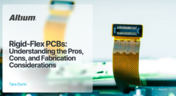
Rigid-Flex PCBs: Understanding the Pros, Cons, and Fabrication Considerations
Read our new article which discusses the advantages of rigid-flex PCBs, such as space-saving designs and enhanced reliability, while also addressing potential challenges in their fabrication. It provides essential design and manufacturing tips to help engineers effectively implement this technology in various applications.


Your search returns no results.


