News & Updates

NEW

Blog
•
How Design Review Automation Saves Hours (and Headaches) Per Project
Design review automation helps teams spend less time managing feedback and more time improving the design. This article explores how centralized comments, structured checklists, action tracking, and approval workflows can make reviews faster, more consistent, and easier to close.

NEW

Blog
•
Comparing Flex and Rigid-Flex PCBs: When to Use What?
This article compares flex and rigid-flex PCBs across key design and manufacturing considerations, including cost, bend radius, impedance, and assembly complexity. It explains how choosing the right construction early can help reduce design risks and ensure better manufacturability.


Blog
•
The Security and Speed of Cloud-Based Electronics Design for Engineering Teams
Security shouldn't be the reason your engineering team slows down. This article explores how cloud-based design platforms can turn secure access, governance, and IP protection into an enabler of faster collaboration rather than another development bottleneck.


Blog
•
PCB Assembly Outputs
The right PCB assembly outputs turn a finished design into a buildable product. This article covers the essential manufacturing files and DFA considerations that help ensure assemblers have the information they need for accurate, reliable production.


Blog
•
Holistic Engineering Management in Electronic Design
This webinar explores how engineering leaders can gain greater visibility and control across complex electronic design workflows. Discover how connected processes and centralized design data help teams reduce risk, improve collaboration, and deliver projects on time.

Blog
•
PCB Design Variants: Managing Multiple PCBA Versions
Product variations often require different component populations, alternate parts, or configuration settings while keeping the underlying PCB design unchanged. This article explains how structured variant management keeps these differences organized and ensures each configuration has the correct BOM and manufacturing outputs.


Blog
•
8 Common DFM Problems PCB Design Rules Catch Before Fab
Preventing DFM problems starts before fabrication not during the fab review. This article covers eight common PCB manufacturing issues and the design rules that help engineers identify and resolve them early.


Blog
•
What is a Multi-CAD Environment? Advantages and Best Practices
Different CAD tools shouldn't mean disconnected teams. Learn how Multi-CAD workflows help engineers review designs, collaborate across disciplines, and catch mechanical or sourcing issues before they become costly redesigns.

Blog
•
Deliver Production-Ready Multiboard PCBs Faster with Manufacturing-Driven Design
This article explores how manufacturing-driven design can help teams validate multiboard products before they reach the factory. It highlights how early checks of interconnects, harnesses, mechanical fit, sourcing, and manufacturing data can reduce late-stage changes and accelerate production readiness.


Blog
•
Stop Chasing Signatures: How Automated Design Sign-offs Accelerate Release Cycles
Automated design sign-offs can eliminate much of the administrative friction surrounding hardware approvals. This article explores how in-context reviews, structured workflows, and automated traceability help teams accelerate release cycles while maintaining control.

Blog
•
Altium Designer 22.6 Update
We are happy to announce that the Altium Designer 22.6 update is now available. Altium Designer 22.6 continues to focus on improving the user experience, as well as performance and stability of the software, based on feedback from our users. Check out the key new features in the What's New section on the left side of this window!

Blog
•
Join PCB Design Review Competition from Altium
Find 9 mistakes in a PCB design and get added into the lucky draw to win a prize from Altium!

Blog
•
SAP (Semi-Additive PCB Process) – Top 5 Questions Regarding Stack Up
This Semi-Additive Process is an additional tool in the PCB fabricators' toolbox that enables them to provide feature sizes for trace width and spacing that are 25 microns, (1 mil) and below depending on the fabricators' imaging equipment. This provides much more flexibility to breakout out tight BGA areas and the ability to shrink overall circuit size and/ or reduce the number of circuit layers in the design. As the PCB design community embraces the benefits of this new printed circuit board fabrication technique, there are of course many questions to be answered.

Blog
•
Improving Supply Chain Success with BOM Management
It’s no secret that component shortages have become more frequent this year. In fact, countries around the world are losing billions in revenue due to supply issues. Having the right components on hand is more crucial than ever as availability, obsolescence, counterfeit products and environmental non-compliance risks continue to grow. Fortunately, many shortages can be avoided by introducing proactive supply chain practices.
Blog
•
What is the Impedance of Length-Tuning Structures?
Do length-tuning structures create an impedance discontinuity? The answer is an unequivocal “yes”, but it might not matter in your design depending on several factors. Applying a length-tuning structure is equivalent to changing the distance between the traces while meandering. Therefore, you will have a change in the odd-mode impedance of a single trace. The question then becomes: does this deviation in trace impedance in a length tuning structure matter?

Blog
•
A-SAP™ – What do you need to know?
The continued miniaturization of both packaging and component size in next-generation electronics is becoming harder and harder to work around and presents a significant challenge for both PCB designers and PCB fabricators. To effectively navigate the constraints of the traditional subtractive-etch PCB fabrication processes, PCB designs require advanced PCB fabrication capabilities while pushing the limits of finer feature size, higher layer counts, multiple levels of stacked micro vias and increased lamination cycles.

Blog
•
Pin-Package Delay and Via Delay in High Speed Length Tuning
Take a look at the inside of some integrated circuit packages, and you’ll find a number of wires bonded to the semiconductor die and the pads at the edge of the component's package. As a signal traverses makes its way along an interconnect and into a destination circuit, signals need to travel across these bond wires and pads before they are interpreted as a logic state. As you look around the edge of an IC, these bond wires can have different lengths, and they incur different levels of delay and contribute to total jitter.

Blog
•
6-Layer PCB Design Guidelines
Once you’ve run out of room on your 4-layer PCB, it’s time to graduate to a 6-layer board. The additional layer can give you room for more signals, an additional plane pair, or a mix of conductors. How you use these extra layers is less important than how you arrange them in the PCB stackup, as well as how you route on a 6-layer PCB. If you’ve never used a 6-layer board before, or you’ve had EMI troubles with this stackup that are difficult to solve, keep reading to see some 6-layer PCB design guidelines and best practices.
Blog
•
Altium Designer 22.5 Update
We are happy to announce that the Altium Designer 22.5 update is now available. Altium Designer 22.5 continues to focus on improving the user experience, as well as performance and stability of the software, based on feedback from our users. Check out the key new features in the What's New section on the left side of this window!

Blog
•
How Reliable is Your Hybrid PCB Stackup?
PCB stackups often incorporate slightly dissimilar materials that could pose a reliability problem. Hybrid PCBs are one case where the PCB stackup will include different materials, typically a standard FR4 laminate and a PTFE laminate for RF PCBs. Designers who want to take the lead on material selection when designing their hybrid stackups should consider these factors that affect reliability. As with any PCB stackup, make sure you get your fabricator involved in the manufacturing process early to ensure reliability problems do not arise during production.

Blog
•
Monte Carlo Simulation vs. Sensitivity Analysis: What’s the Difference?
In a previous article about circuit simulation and reliability, I looked at how Monte Carlo analysis is commonly used to evaluate circuits that are subject to random variations in component values. Sensitivity analysis is a bit different and it tells you how the operating characteristics of your circuit change in a specific direction. Compared to a Monte Carlo simulation, sensitivity analysis gives you a convenient way to predict exactly how the operating characteristics will change if you were to deliberately increase or decrease the value of a component.

Blog
•
Creating Continuous Integration Pipelines for FPGAs
Field Programmable Gate Arrays, or FPGAs, have become ubiquitous amongst high-speed, real-time digital systems. The speed at which FPGAs operate continues to increase at a dizzying pace but their adoption into Continuous Integration pipelines seems not to trail as closely. In this article we will review the concept of CI pipelines, their application to FPGAs, and look at examples on how to set this up.
Blog
•
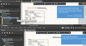
Soft Locks [Conflict Prevention] in Altium 365
Conflicts can occur when multiple people work on the same project simultaneously. The user might not realize that they are not looking at the latest version of the documentation, leading to problems later. To address this issue, Altium features an intuitive graphical user interface that allows you to examine conflicts quickly and carefully

Blog
•
The Basics of Monte Carlo in SPICE: Theory and Demo
Anytime you place a component in your PCB, it’s almost like you’re gambling. All components have tolerances, and some of these are very precise, but others components can have very wide tolerances on their nominal values. In the event the tolerances on these components become too large, how can you predict how these tolerances will affect your circuits?

Blog
•
What's In Your BGA Land Pattern and Footprint
If you look in datasheets for most components, you’ll often find a recommended land pattern, usually alongside some mechanical package information and assembly information. This is not always the case with BGA components, especially components with high ball count. There are a few reasons for this that we can speculate: those ball counts might just be too big to put into a single page, or the manufacturer just expects you to know how to create that land pattern.

Blog
•
MIDs Make a Comeback as Vertical SMD Modules for Your PCB
Molded interconnect devices are essentially plastic molded substrates with traces running along any surface, including at right angles and running vertically. Altium users can use the new 3D Routing extension to design their own component carriers, which can be mounted vertically in a standard assembly process. If you’ve always wanted to vertically mount components or entire circuits, but without the expense of adding a flex section to your design, the new 3D Routing extension with HARTING’s component carrier designs provides a unique solution.



On-Demand Webinar
•
Jun 12, 2025
Proactive Lifecycle Management: Preventing Obsolescence Before It Hits


On-Demand Webinar
•
Apr 23, 2025
Collaborative Design Review: Ensuring Quality from Schematics to Supply Chain

On-Demand Webinar
•
Apr 22, 2025
From Prototype to Production: Optimizing BOM Costs Without Compromising Quality with Part Analytics


On-Demand Webinar
•
Apr 9, 2025
Component Selection in Altium Designer: Making Data-Driven Decisions with Data Integrations

On-Demand Webinar
•
Mar 25, 2025
Unlocking the full potential of your design team with Altium's enterprise solution


On-Demand Webinar
•
Jan 24, 2024
Discover How Altium Designer 24 Revolutionizes Team Dynamics in PCB Design


