Welcome, Guest

Sign in to learn, create, and do more with the product you love.

News & Updates

Filters:
Tag
NEW
Embedded thumbnail for Add Unit-Aware Temperature Coefficient Parameters
New in Altium's Software
Add Unit-Aware Temperature Coefficient Parameters

Component templates in a connected Workspace on the Altium Platform now include support for Temperature Coefficient (ppm/°C) as a unit-aware user parameter type. This makes it possible to define temperature coefficient values directly within the template using the appropriate units.

NEW
Embedded thumbnail for When to Add Part Numbers to SMD Passives
How-To's
When to Add Part Numbers to SMD Passives

Check out our new video covering essential electronics fundamentals, with a focus on why including part numbers for SMD passive components, such as SMD resistors, directly on schematics is so important. We also explore whether relying only on the Bill of Materials (BOM) is enough for effective electronic component management.

NEW
Blog
Complex Engineering Projects Leverage Multiple ECAD/MCAD Formats

This article explores how modern engineering teams manage complex projects involving multiple ECAD, MCAD, and manufacturing file formats across distributed workflows. It highlights the importance of design authority, disciplined revision control, and bidirectional collaboration to ensure accurate integration between PCBs and mechanical systems.

Embedded thumbnail for Present Large Harness Tables More Clearly
New in Altium's Software
Present Large Harness Tables More Clearly

Harness Draftsman now supports splitting connection tables across multiple pages in *.HarDwf documents. With the new page height limit setting, you can easily control how much of the table appears on each page.

Embedded thumbnail for Innovate Beyond - The Future of Electronics Development in Automotive
How-To's
Innovate Beyond - The Future of Electronics Development in Automotive

Discover how the future of automotive electronics is being shaped by a more connected development approach that unifies teams, data, requirements, design, collaboration, and manufacturing. Recorded at BMW Welt and the BMW Museum during Altium’s "The Future of Electronics Development in Automotive" event, this video explores the key challenges and innovations driving the next generation of automotive design.

Blog
BOM Cost Optimization During Schematic Capture

Engineering and sourcing teams work best when BOM decisions happen with live market data in view. This article explains how integrated cost and availability insights help teams collaborate earlier and avoid redesigns driven by supply chain issues.

Embedded thumbnail for Coming Soon: Design Rule Sets
New in Altium's Software
Coming Soon: Design Rule Sets

Soon, PCB design rules in Altium will be organized into reusable Rule Sets within the PCB Rules and Constraints Editor. These rule sets can be created, duplicated, enabled or disabled, renamed, deleted, imported, and exported, making it easier to manage rules for specific interfaces, manufacturing requirements, or unique design constraints.

Embedded thumbnail for Decoupling Capacitor Routing: When to Use Vias vs Traces
How-To's
Decoupling Capacitor Routing: When to Use Vias vs Traces

Check out this video, a follow-up to the decoupling capacitor placement series, exploring the inductance tradeoffs between trace routing and via connections. Using real component examples from an Ethernet switch design in Altium, the video demonstrates how different routing choices can impact overall performance.

Embedded thumbnail for Coming Soon: Interactive Dynamic Phase Tuning
New in Altium's Software
Coming Soon: Interactive Dynamic Phase Tuning

The Interactive Length Tuning tool allows you to manually tune a single net in a differential pair while maintaining equal pair length and phase alignment across the entire route. This enables more efficient differential signal transmission, greater control during manual tuning, and faster pattern creation within defined phase tolerance limits.

Blog
How to Use a Multicad Viewer for Seamless Collaboration

Because ECAD formats are typically incompatible, teams often struggle with versioning, conversions, and fragmented review processes. This article breaks down how multi-CAD viewers provide a unified, read-only environment that supports structured design reviews, comments, and task assignment across disciplines.

Embedded thumbnail for AI PCB Layout vs. Human Design: The Honest Truth
How-To's
AI PCB Layout vs. Human Design: The Honest Truth

The question is: Can AI really route a PCB as well as an experienced human designer? In this video, we set out to find the answer. Our expert, Zach Peterson, puts it to the test in a side-by-side layout review. The challenge is based on a LinkedIn post where viewers had to guess which board was AI-generated and which was designed by a human.

Embedded thumbnail for Improve Your 3D Wire Bonding Workflow
New in Altium's Software
Improve Your 3D Wire Bonding Workflow

Check out the video where we showcase enhanced wire bonding features, including precise bond wire shape definition, improved clearance checking, streamlined import and export workflows, and efficient management of wire bonding objects.

Blog
Rigid-Flex PCBs in Consumer Electronics

Rigid-flex PCBs help modern devices get smaller, lighter, and more compact by eliminating connectors and fitting into tight 3D spaces. This article explains how to design them properly to avoid common reliability issues.

Blog
From Design to First Assembly: Complete Your BOM & Plan Your Build

This webinar walks through the complete post-release workflow, from generating a managed BOM to sourcing components and assembling the first prototype. It demonstrates how integrated tools streamline data enrichment, supplier selection, and guided assembly to reduce delays and errors.

Blog
The Future of BOM Management: Trends and Innovations

BOM management is no longer just a checklist. It’s becoming a real-time engine for smarter decisions! Discover how AI, automation, and connected systems are transforming BOMs into powerful tools for navigating supply chain uncertainty.

Tag
Broken PCB
Blog
The High-Reliability PCBA Design and Test Challenge

High-reliability electronics must go through multiple rounds of testing and qualification to ensure they can withstand their intended operating environment. Designing to performance standards, whether the baseline IPC standards or more stringent industry standards, is the first step in ensuring a reliable circuit board. In this e-book, readers will gain a thorough look into PCB testing and analysis, starting from basic tests performed on bare boards and completed assemblies.

Where to place AC Caps on PCIe Lanes
Blog
AC Coupling Capacitors in PCIe Routing

Coupling capacitors find plenty of uses in analog applications and on differential protocols, acting essentially as high pass filters that remove DC bias carried seen on a signal. In the case of PCIe, there are a few reasons to place AC coupling capacitors on differential pairs beyond the fact that AC coupling capacitors are listed in the standard. In this article, we’ll look briefly at where to place coupling capacitors on PCIe links, as well as the reasons these are placed on PCIe links.

Tuning dialog
Blog
Altium Designer 22.7 Update

We are happy to announce that the Altium Designer 22.7 update is now available. Altium Designer 22.7 continues to focus on improving the user experience, as well as performance and stability of the software, based on feedback from our users. Check out the key new features in the What's New section on the left side of this window!
The Positive Impact of Supply Chain Visibility on Design to Cost
Blog
The Positive Impact of Supply Chain Visibility on Design to Cost

Design to cost is a lofty idea that is only perfectly executed when supply and demand for components are in perfect harmony. Unfortunately, the current landscape for component sourcing makes design to cost more of a balancing act rather than an exercise in price reduction. To help designers in their efforts to balance cost, capabilities, and procurement, we created this ebook to help users understand how modern supply chain tools can help in these complex design problems.

Evaluating Stubs on PCIe Lanes
Blog
A Brief Study of Stubs on a PCIe Connector

Stubs are an important topic in high-speed PCB design, and there is a longstanding guideline that stubs should always be removed from all vias on high-speed digital interconnects. While stubs are bad for high-speed lines, they do not always need to be removed. What is more important is to predict the loss profile and frequencies, and to floorplan appropriately to try and prevent such losses.

Surface Layer DFM and Cleanup
Blog
PCB Layout Cleanup Before Manufacturing

Once you finish your placement and routing in your PCB layout, it can be tempting to wrap up the layout and send everything in directly to manufacturing. The reality is that the board may still need some work before it is considered finished. The cleanup you perform at the final stage of PCB layout will help you catch any outstanding errors that can't be programmed into your DRC engine, and it gives you a chance to add any outstanding details to the surface layers.

Low Cost and Professionally Built LED Panel
Blog
Insulated Metal Substrates: Building an LED Panel

In this project we’ll be building a moderate sized LED panel on insulated metal substrate (IMS). This light panel has three different white balance High CRI LED types on it, warm, neutral and cool. By changing the brightness of the different white balances, the light from the panel can be adjusted to match other lighting, making it perfect for film use - but also creating perfect lighting for electronics work. As with all my projects, this LED panel is open source, you can find the Altium project files over on my GitHub released under the permissive MIT License.

DFM For Your Materials
Blog
DFM in PCB Material Selection

Every design should begin with selecting the materials that will appear in the PCB stackup, as well as arranging layers in the stackup to support layout and routing. This section of our PCB manufacturing andc DFM crash course focuses on selecting the right materials for your PCB design. Materials should be selected given the particular design requirements outlined in your specifications.

PCB Layout for an BGA
Blog
How to Start an FPGA PCB Layout For Your Embedded System

FPGAs come in quad or BGA packages that can be difficult to floorplan, especially with the high number of I/Os often implemented in these components. FPGAs offer a lot of advantages in terms of their reconfigurability, but they can require a lot of effort to layout and route without headaches. If you’ve never worked with an FPGA in your PCB layout, we have some guidelines that can help you get started.

2-port VNA on a 3-port Network
Blog
How to Get 3-port S-parameters From a 2-port VNA Measurement

S-parameters are fundamental quantities in signal integrity, and an ability to understand them from measurement or analysis is very important. If you have a 3-port network, like a power divider or circulator, it may appear that you must use a 3-port VNA to measure these S-parameters. It is always acceptable to measure between two ports, but you need to know what exactly it is you are measuring. In this article, we’ll look at the relationship between the true 3-port S-parameters with a 2-port measurement.

Fab and Assembly Crash Course
Blog
A Day in the Life of the PCB Manufacturing Process

Before implementing design for manufacturing, it is important to understand the underlying process behind producing a physical PCB. Regardless of the various technologies present in each facility, a large majority of industry-leading manufacturers follow a specific set of steps to turn your design from a drawing in a CAD application into a physical board. In this article, we'll cover the basics that designers need to know as part of our crash course series on PCB manufacturing.

What Are the Main Skew Sources in a PCB?
Blog
Addressing Skew Sources in High Speed PCBs

If you compile a list of skew sources, you'll see that fiber weave-induced skew is only one entry on a long list of skew sources. We'll look at this list of possible skew sources below, and we'll see how they affect the operation of your PCB. From the list below, we'll see that some of these issues with skew are not simply solved by paying attention to the fiber weave construction in a PCB substrate.

Ground Below SMPS Inductors
Blog
Should Ground Be Placed Below Inductors in Switching Regulators?

We love answering questions from our readers and YouTube viewers, and one of the recent questions we received relates to EMI from switching elements in a switching regulator is "Should a cutout be placed below the inductor in a switching regulator circuit?". Despite the variations in inductors and their magnetic behavior, there are some general principles that can be used to judge the effects of placing ground near inductors in switching regulator circuits. We’ll look at some of these principles in this article

Alternative Pins
Blog
Altium Designer 22.6 Update

We are happy to announce that the Altium Designer 22.6 update is now available. Altium Designer 22.6 continues to focus on improving the user experience, as well as performance and stability of the software, based on feedback from our users. Check out the key new features in the What's New section on the left side of this window!

Top 5 Questions Regarding Stack Up
Blog
SAP (Semi-Additive PCB Process) – Top 5 Questions Regarding Stack Up

This Semi-Additive Process is an additional tool in the PCB fabricators' toolbox that enables them to provide feature sizes for trace width and spacing that are 25 microns, (1 mil) and below depending on the fabricators' imaging equipment. This provides much more flexibility to breakout out tight BGA areas and the ability to shrink overall circuit size and/ or reduce the number of circuit layers in the design. As the PCB design community embraces the benefits of this new printed circuit board fabrication technique, there are of course many questions to be answered.

Tag
Embedded thumbnail for Happy Holidays!!!
How-To's
Happy Holidays!!!

Altium sending you warm wishes for Christmas filled with all the things that bring you joy, surrounded by the people you love and may your dreams blossom and make all your aspirations come true in the coming year.

Embedded thumbnail for Harness Design in Altium Designer helps Lazer Lamps built better products faster
Success Stories
Harness Design in Altium Designer helps Lazer Lamps built better products faster

Hear the story of how Altium Designer's Harness Design feature streamlines wiring system design to empower Lazer Lamps’ engineering team to craft superior LED driving lights in record time. From seamless collaboration among their engineering teams to the intuitive design features that accelerated their workflows, witness firsthand how Altium Designer helped improve Lazer Lamps design processes.

Embedded thumbnail for Altium Designer 24 - Out Now!
New in Altium Designer 24
Altium Designer 24 - Out Now!

Altium Designer 24 has arrived, heralding a groundbreaking transformation. Now available for download, it introduces exciting features including PCB CoDesign, Constraint Manager, PCB Layout Replication, Ansys CoDesigner and much more. Altium Designer isn't just a requested tool; it's a requirement that establishes the standard in electronic design.

Embedded thumbnail for Coming Soon: Sectional View
New in Altium Designer 24
Coming Soon: Sectional View

Discover more about our latest upgraded feature, premiering on December 13th. The Sectional View is a tool that simplifies and enhances your PCB design process. Whether you're troubleshooting complex designs or streamlining your workflow, it provides clarity and efficiency.

Embedded thumbnail for Coming Soon: Advanced Mixed Simulation Features
New in Altium Designer 24
Coming Soon: Advanced Mixed Simulation Features

We invite you to explore the world of mixed simulation. Delve deeper into key information about this feature and its enhanced functionalities, available starting December 13th. Set up mixed-signal simulations to ensure accuracy and reliability in your design testing

Embedded thumbnail for Coming Soon: Harness MCAD CoDesign
New in Altium Designer 24
Coming Soon: Harness MCAD CoDesign

In this short video, you can explore how Harness MCAD CoDesign, available on the 13th of December, streamlines the design process by minimizing errors, accelerating iterations, and ensuring a synchronized development process. Altium Designer 24 is on the horizon, and it's not just a request but a requirement for optimizing your electronic design process.

Embedded thumbnail for Altium Designer 24: From Requested to Required
New in Altium Designer 24
Altium Designer 24: From Requested to Required

Altium Designer 24 is getting closer! In this short video, we are presenting a list of new features and improvements that will be available starting from the 13th of December in our software.

Embedded thumbnail for Coming Soon: Harness Multi-Board
How-To's
Coming Soon: Harness Multi-Board

Altium Designer's all-in-one approach to electronic design seamlessly combines Harness and Multi-Board Design capabilities, allowing you to create complex multi-board systems with ease. This new feature, available from December 13th, provides an opportunity to bring design and manufacturing teams together, inspiring a streamlined design process, reducing the risk of errors, and ensuring unwavering project deliveries.

Tackle Any Design Complexity With the Constraint Manager
What's New in 23.11
Tackle Any Design Complexity With the Constraint Manager

For enterprise and pro subscriptions, the new Constraint Manager offers a table-based interface, accessible from both Schematic and PCB, allowing you to define constraints more collaboratively. Engineers and stakeholders can collectively set design constraints with ease.

Tackle Any Design Complexity With the Constraint Manager
What's New in 23.11
使用约束管理器应对任何设计复杂性

对于企业版和专业版订阅用户,新约束管理器提供了基于表格的界面,无论从原理图还是 PCB 都可以访问,帮助您加强在约束定义方面的协作力度。工程师和协作者都可以轻松地共同设置设计约束。

Embedded thumbnail for Minimize Manual Effort With Automatic Length Tuning
What's New in 23.11
Minimize Manual Effort With Automatic Length Tuning

Automatic Length Tuning introduces automatic length and delay tuning functionality in 2D mode, accessed conveniently from the main Route menu. This feature reduces the manual effort typically associated with length and delay tuning, expediting your design process.

Embedded thumbnail for Minimize Manual Effort With Automatic Length Tuning
What's New in 23.11
通过自动长度调整功能来减少手动操作

自动长度调整提供 2D 模式下的自动长度调整和延迟调整功能,可方便地从主布线菜单访问。该功能可以减少进行长度调整和延迟调整时通常需要的手动操作,从而加快设计进程。

Embedded thumbnail for The Most Common 2-Layer PCB Design Mistakes and How To Avoid Them
How-To's
The Most Common 2-Layer PCB Design Mistakes and How To Avoid Them

Do you encounter issues when preparing a two-layer board? In this video, we address some of the most common mistakes made with this type of board and explain why upgrading to a four-layer board might be the solution you need.

Embedded thumbnail for Coming Soon: Ansys CoDesigner
How-To's
Coming Soon: Ansys CoDesigner

Ansys CoDesigner (which will be released on the13th of December) simplifies your design process by connecting ECAD and Simulation to eliminate manual export/import steps. With features like design change synchronization and commenting, Altium Designer ECAD engineers and Ansys Electronics Desktop (AEDT) SIM engineers can collaborate seamlessly in one workspace.

Embedded thumbnail for Coming Soon: Automatic Multi-Net Tuning
How-To's
Coming Soon: Automatic Multi-Net Tuning

Automatic Multi-Net Tuning enhances PCB design accuracy and efficiency by automatically adjusting multiple nets simultaneously to meet specific design rules, including length and delay. Learn more about this feature, which will be released on December 13th. Its flexibility enables effective work with differential pairs and traces at any angle. It not only identifies but also rectifies issues related to automatic length tuning, ensuring your designs adhere to key standards without the need for manual adjustments.

Embedded thumbnail for Coming Soon: PCB CoDesign
How-To's
Coming Soon: PCB CoDesign

PCB CoDesign makes it easier for everyone to work together and meet project deadlines. In Altium Designer 24, which is scheduled for release on December 13th, we are introducing a new feature. This feature optimizes your resources through a Git-like approach, allowing multiple team members to work simultaneously and commit changes to a master branch. This expedites the design process and lowers project costs.

Tag
Integrating Requirements June 2025 Webinar
On-Demand Webinar May 28, 2025
Integrating Requirements into Your PCB Design Workflow
Join our webinar where you will learn about integrated requirements tools who can help you eliminate late-stage design changes, AI support through system requirements and integration of design requirements directly in PCB Design. Don't miss it, register now!
Streamlining Team Collaboration
On-Demand Webinar Apr 17, 2025
Streamlining Team Collaboration in Industrial PCB Projects
Join us for our upcoming webinar to discover how Altium Designer and Altium 365 can transform your team’s collaboration and take your PCB design projects to the next level. Attend for a chance to win free access to the Altium 365 Training Bundle.
PCB CoDesign Webinar
On-Demand Webinar Jan 24, 2024
Discover How Altium Designer 24 Revolutionizes Team Dynamics in PCB Design
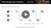
Expand your collaboration skills and stay ahead of the curve with PCB CoDesign. Design teams often grapple with prolonged design cycles and coordination issues, leading to delays and inefficiencies. In the current landscape, design processes are hindered by fragmented collaboration, resulting in increased layout times and difficulties in synchronizing design updates.