Welcome, Guest

Sign in to learn, create, and do more with the product you love.

News & Updates

Filters:
Tag
NEW
Blog
How to Design a PCB: From Schematic Capture to Manufacturing

This article walks through the complete PCB design workflow, from schematic capture and component selection to layout, design reviews, and manufacturing documentation. It highlights the key decisions at each stage that help engineering teams produce reliable, manufacturable products.

NEW
Embedded thumbnail for Future of Electronics Development in Security and Aerospace
How-To's
Future of Electronics Development in Security and Aerospace

See the highlights from Altium's executive event in Hamburg, where Security and Aerospace leaders explored AI-driven development, digital engineering, supply chain resilience, and the future of mission-critical electronics.

NEW
Blog
5 Power Integrity Myths: AC Edition

The biggest threat to your power integrity might be outdated design advice. This article challenges five common AC power integrity myths and shows what really matters when designing today's high-speed PCBs.

NEW
Embedded thumbnail for Create Clearance Rules Faster and with Less Effort
New in Altium's Software
Create Clearance Rules Faster and with Less Effort

Setting up clearance rules is now more intuitive in the Constraint Manager. Choose the Simple view for faster configuration with grouped object types, or the Advanced view when you need detailed, matrix-based clearance control.

Blog
Your Design Data Has Zero Defense

Your design data may be more exposed than you think. This webinar shows how to identify common security gaps and secure engineering workflows with centralized access control and governance.

Embedded thumbnail for Mastering HDI Design Rules in Altium Designer
How-To's
Mastering HDI Design Rules in Altium Designer

In our latest Altium Academy tutorial, we guide you through configuring the essential HDI PCB design rules in Altium's software. You'll learn how to use your manufacturer's fabrication capabilities to create accurate design rules and constraints for your PCB.

Embedded thumbnail for Search, Filter, and Navigate PCB Designs Faster
New in Altium's Software
Search, Filter, and Navigate PCB Designs Faster

The Web Viewer now features a redesigned search experience for faster access to PCB design data across supported CAD formats. A lightweight, intuitive interface lets you begin with simple search terms and progressively refine results using contextual suggestions.

Blog
Integrated PCB Design vs. Legacy Point Tools: What’s the Real Cost?

As hardware development grows more collaborative, disconnected point tools can introduce data inconsistencies, traceability gaps, and costly coordination challenges. This article examines how integrated PCB design environments connect design, mechanical, supply chain, and review workflows to improve efficiency throughout the product lifecycle.

Blog
Make Better Design Decisions with Signal and Power Integrity Insight

Signal integrity and power integrity are closely connected, with problems in one often affecting the other as designs become faster and more complex. This webinar explains how integrated analysis workflows help engineers evaluate PDN performance, identify potential issues early, and improve overall design quality.

Embedded thumbnail for Gain Better Control Over Wire Bond Visibility
New in Altium's Software
Gain Better Control Over Wire Bond Visibility

New bond wire visibility controls give you greater flexibility when working with wire-bonded boards and footprints, making it easier to focus on the details that matter most.

Embedded thumbnail for Coming Soon: Selectable Harness Source Within Multi-board Design
New in Altium's Software
Coming Soon: Selectable Harness Source Within Multi-board Design

Selectable Harness Source Within Multi-board Design enables harness projects to drive system connectivity while maintaining bidirectional synchronization between multi-board schematics and harness wiring diagrams for improved accuracy and easier design management.

Embedded thumbnail for Choose the Simbeor Version for Your PCB Calculations
New in Altium's Software
Choose the Simbeor Version for Your PCB Calculations

The PCB Editor now lets you choose the Simbeor version used for delay and impedance calculations, giving you more flexibility and consistency across your design workflows.

Blog
Agile Teams: From Design Tool to Product Development Platform

Learn how Agile Teams evolves beyond traditional PCB design workflows to support connected product development. This webinar explores how centralized data, collaboration tools, and governance capabilities help teams accelerate delivery while maintaining control.

Embedded thumbnail for Improve PCB Editor Performance with Via Instancing
New in Altium's Software
Improve PCB Editor Performance with Via Instancing

The PCB Editor now uses via instancing to generate geometry for each via individually, providing greater flexibility and a more advanced approach to managing vias in PCB designs.

Tag
How To Import Libraries and Manage Components With Altium 365
Blog
How To Import Libraries and Manage Components With Altium 365

The problems you can experience with components and libraries are endless. These problems are the most significant source of design issues and the biggest reason behind respins, costing companies untold amounts of lost profit annually.
If you want to have a better understanding of how to use Altium 365 to maintain a strong and centralized library that is free of problems and headaches, you may want to consider attending this lecture.

The High-Speed PCB Stackup Design Challenge
Blog
The High-Speed PCB Stackup Design Challenge

As much as we would like to build every high speed PCB perfectly, with ideal SI/PI/EMI characteristics, it isn’t always possible due to many practical constraints. Sometimes a stackup can be “good enough,” even for a high-speed PCB. This always comes from the need to balance engineering constraints, functional requirements, and the need to ensure signal and power integrity in a high-speed design, and finally to ensure compliance with EMC requirements.

How I Improved My Collaboration Efficiency with Altium 365
Blog
How I Improved My Collaboration Efficiency with Altium 365

Involving the whole team that will bring a product to completion early on in the development cycle is vital to efficient development. Design reviews with all the relevant parties are critical at each step of the design process, starting with high-level component selection, then through the schematic capture and PCB layout stages. 

Countersink and Counterbore
Blog
Countersink and Counterbore

Ergonomics and convenience are important issues when designing a printed circuit board and the device as a whole. A lot of Altium Designer tools are aimed at solving them. These include Countersink and Counterbore holes, which allow the use of various types of screws in the mounting holes of the board.

Migrating Data From Other Version Control Systems
Blog
Migrating Data From Other Version Control Systems

The development of electronic devices always involves the release of many different types of files. And these files are not static - they change as the project progresses. When filling a project with data, a user creates new files, modifies outdated files that have become irrelevant. Managing project data is a separate task, especially for large developments where several participants with different specializations are involved in the process.

Properties Panel Tuning
Blog
Properties Panel Tuning

High-speed PCBs often require tuning groups of tracks, both single and differential. Altium Designer includes powerful tools that allow you to solve such tasks quickly and with high quality. Study this document and achieve the desired result even faster.

Reflectionless Matching vs. Conjugate Matching: An Apparent Contradiction
Blog
Reflectionless Matching vs. Conjugate Matching: An Apparent Contradiction

There is one confusion related to impedance matching that comes up again and again, and it appears to be a fundamental confusion between reflection and power delivery. This leads to an apparent contradiction that arises when we try to generalize power delivery to wave reflection, despite the fact that the two were not meant to be related.

Properties Panel Routing
Blog
Properties Panel Routing

Routing is one of the most time-consuming stages of PCB design. Altium Designer has a large set of tools that allow you to do it as accurately and quickly as possible. This document will help you to learn how to manage your routing effectively and use it to its fullest extent.

Quarter-Wave Transformer Design For Real and Reactive Loads
Blog
Quarter-Wave Transformer Design For Real and Reactive Loads

RF systems operate with specific impedance values across entire interconnects, including on PCBs. Not all RF components are packaged in integrated circuits with defined impedances, so impedance matching circuits and line sections are needed to ensure signal transmission between different sections of an interconnect. One of these impedance matching techniques is the quarter-wave impedance transformer, which can be implemented as a printed trace with specific impedance.

Schematic
Blog
Altium Designer 22.10 Update

We are happy to announce that the Altium Designer 22.10 update is now available. Altium Designer 22.10 continues to focus on improving the user experience, as well as performance and stability of the software, based on feedback from our users. Check out the key new features in the What's New section on the left side of this window!

Component Warpage Causes in a PCB
Blog
Component Warpage Causes in a PCB

A staff member at a PCB manufacturer once explained to me that they thought we were having an issue with a package warping. Unfortunately, component warping can occur both in a PCB and in components. In this article, we'll give an overview of warpage in a PCB, specifically in the circuit board and in the components.

Link Budget Calculator
Blog
RF Signal Chain and Link Budget Basics

If you're designing a wireless IoT device, and you know how to calculate the link budget, you can reasonably estimate whether your signal will reach its destination and be read by the receiver. To calculate the link budget, the designer needs to know something about all other sources of gain and loss in the system. Once link budget is determined, the designer can judge whether some modification is needed in their RF signal chain. 

How to Calculate SMD Pad Sizes?
Blog
Best Methods for Calculating SMD Pad Size in PCB Design

SMD components require precisely sized pads for soldering during assembly. The designer is responsible for ensuring pad sizes are correct, either by calculating them and comparing with footprint data, looking through datasheets, or by memorizing SMD pad size standards. If you have a component and you don't have access to the footprint, and you decide to biuld the footprint yourself, what resources are available to ensure you have the correct pad size?

Can You Fix a Warped PCB?
Blog
Can You Fix a Warped PCB?

Before we get too deep into this article, I’ll give you the simple answer. You probably can’t fix warping in your PCB after it’s already been fabricated. You can prevent an unwarped board from becoming warped during assembly, but only as long as materials were selected properly and the board is put into reflow correctly. We’ll run over some of these points in this article, and I’ll examine some points that might help you recover a warped board.

What is an Eye Diagram?
Blog
What is an Eye Diagram?

The eye diagram is a useful measurement or simulation as part of channel compliance. The measurement shows many different factors that can affect signal behavior simultaneously, ultimately allowing for qualification of errors and losses in a channel. In this article, I’ll run over some of the fundamental measurements that you could manually extract from an eye diagram and how they reveal some strategies for improving channel designs.

Skills for Today's PCB Designers
Blog
What Skills Are Needed to be a PCB Layout Designer?

To readers who have been working in the PCB industry for most of your career, you have probably seen a very diverse group of professionals with varied skill sets and backgrounds. Designers might get started as engineers or as technicians, and some designers learn how to create beautiful PCB layouts in university. No matter how you got into PCB design, there are some important skills to know that will take you a long way towards advancing your career.

Tag
Embedded thumbnail for Coming Soon: Interactive Dynamic Phase Tuning
New in Altium's Software
Coming Soon: Interactive Dynamic Phase Tuning

The Interactive Length Tuning tool allows you to manually tune a single net in a differential pair while maintaining equal pair length and phase alignment across the entire route. This enables more efficient differential signal transmission, greater control during manual tuning, and faster pattern creation within defined phase tolerance limits.

Embedded thumbnail for AI PCB Layout vs. Human Design: The Honest Truth
How-To's
AI PCB Layout vs. Human Design: The Honest Truth

The question is: Can AI really route a PCB as well as an experienced human designer? In this video, we set out to find the answer. Our expert, Zach Peterson, puts it to the test in a side-by-side layout review. The challenge is based on a LinkedIn post where viewers had to guess which board was AI-generated and which was designed by a human.

Embedded thumbnail for Improve Your 3D Wire Bonding Workflow
New in Altium's Software
Improve Your 3D Wire Bonding Workflow

Check out the video where we showcase enhanced wire bonding features, including precise bond wire shape definition, improved clearance checking, streamlined import and export workflows, and efficient management of wire bonding objects.

Embedded thumbnail for Customize Your ODB++ Output for Each Partner
New in Altium's Software
Customize Your ODB++ Output for Each Partner

You can now precisely control what design data is included in your ODB++ outputs for different manufacturing recipients. Choose which signal layers to export, decide how the netlist is handled (included, disabled, or neutralized), and control whether component data is removed or shared without properties.

Embedded thumbnail for Proper Voltage Built a Universal Battery Platform with Altium
Altium Stories
Proper Voltage Built a Universal Battery Platform with Altium

Watch our latest customer success story to see how Proper Voltage partnered with Altium to accelerate high-power battery development for next-generation robotics. With our software, they streamlined collaboration, sped up design reviews, improved sourcing visibility, and reduced risk.

Embedded thumbnail for Improve Readability with Custom Pin Spacing
New in Altium's Software
Improve Readability with Custom Pin Spacing

You can now control the vertical spacing of a pin’s designator and name with a custom margin. This setting can be applied globally via Schematic Preferences or adjusted individually in the Pin properties.

Embedded thumbnail for Does Decoupling Capacitor Placement Actually Matter?
How-To's
Does Decoupling Capacitor Placement Actually Matter?

Our new video tackles common questions about capacitor placement on a PCB. Expert Zach Peterson explains why placement is often less critical on multilayer boards with well-designed power and ground planes and shares the key insights most application notes leave out.

Embedded thumbnail for Teaching Power to Think - How Proper Voltage Accelerates Innovation with Altium
Altium Stories
Teaching Power to Think - How Proper Voltage Accelerates Innovation with Altium

Watch the video where you can find how Proper Voltage centralized communication, synchronized ECAD–MCAD development, and gained early insight into supply chain risks using Altium’s connected design platform.

Embedded thumbnail for  Detect Z-Axis Clearance Issues Earlier
New in Altium's Software
Detect Z-Axis Clearance Issues Earlier

The Z-axis clearance rule enables accurate verification of minimum interlayer copper spacing. It supports targeted constraints between net classes, differential pairs, and schematic parameter directives for advanced rule definition.

Embedded thumbnail for Fix Inconsistent Part Parameters in Your PCB Schematic
How-To's
Fix Inconsistent Part Parameters in Your PCB Schematic

Watch our latest video to learn what parameterization really means, why getting the manufacturer name and part number right is essential, and how to quickly identify inconsistencies across your schematic components using Altium’s Parameter Manager tool.

Embedded thumbnail for Create IPC-Aligned Footprints with Less Effort
New in Altium's Software
Create IPC-Aligned Footprints with Less Effort

The default value for the Solder Mask Expansion rule has been updated to improve consistency across design environments. In both PCB documents and rule-driven solder mask expansion within PCB library documents, the default setting is now 0 mil, replacing the previous default of 4 mil.

Embedded thumbnail for Via Dispersion: Why Propagation Delay Changes with Frequency
How-To's
Via Dispersion: Why Propagation Delay Changes with Frequency

Explore the concept of via dispersion and how it impacts propagation delay across frequencies. This tutorial walks through the math behind extracting delay from insertion loss and return loss S-parameters and explains why results can vary depending on your operating range.

Embedded thumbnail for Make Via Rule Configuration More Intuitive
New in Altium's Software
Make Via Rule Configuration More Intuitive

Set precise control over your routing via styles with new rule settings in the Physical View. Define minimum, maximum, and preferred values for both diameter and hole size, and easily switch between constraint ranges or template-based definitions for faster, more flexible design.

Embedded thumbnail for Coplanar Ground Done Right: PCB Design Best Practices
How-To's
Coplanar Ground Done Right: PCB Design Best Practices

When is coplanar ground actually useful and when does it provide no benefit at all? If you’ve ever wondered about this, check out our brand-new video where we tackle one of the most common questions in PCB design.

Embedded thumbnail for Import and Export with Modern Mechanical Models
New in Altium's Software
Import and Export with Modern Mechanical Models

We have expanded mechanical integration by adding support for SOLIDWORKS 2024 and SOLIDWORKS 2025 part models when importing 3D bodies into the design environment. This enhancement allows designers to work with the latest mechanical models created in SOLIDWORKS without the need for additional conversions or workarounds.

Embedded thumbnail for How to Input Via Delay in Altium for DDR Routing
How-To's
How to Input Via Delay in Altium for DDR Routing

In this video, we tackle a real viewer question about DDR3 routing across multiple PCB layers and show how via delay can silently eat into your skew margin before you’ve even finished routing, using Altium’s default 10-layer stackup as a reference.

Tag
Integrating Requirements June 2025 Webinar
On-Demand Webinar May 28, 2025
Integrating Requirements into Your PCB Design Workflow
Join our webinar where you will learn about integrated requirements tools who can help you eliminate late-stage design changes, AI support through system requirements and integration of design requirements directly in PCB Design. Don't miss it, register now!
Streamlining Team Collaboration
On-Demand Webinar Apr 17, 2025
Streamlining Team Collaboration in Industrial PCB Projects
Join us for our upcoming webinar to discover how Altium Designer and Altium 365 can transform your team’s collaboration and take your PCB design projects to the next level. Attend for a chance to win free access to the Altium 365 Training Bundle.
PCB CoDesign Webinar
On-Demand Webinar Jan 24, 2024
Discover How Altium Designer 24 Revolutionizes Team Dynamics in PCB Design
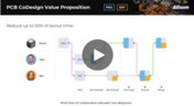
Expand your collaboration skills and stay ahead of the curve with PCB CoDesign. Design teams often grapple with prolonged design cycles and coordination issues, leading to delays and inefficiencies. In the current landscape, design processes are hindered by fragmented collaboration, resulting in increased layout times and difficulties in synchronizing design updates.