News & Updates

Blog
•
Rigid-Flex Stackups: Where Good Designs Go Wrong Before Layout Even Starts
Rigid-flex stackups are more complex than they seem and getting them wrong early can lead to costly failures later. This article shows how smart decisions around materials, transitions, and layer structure help ensure a reliable design.


Blog
•
From Complexity to Clarity: Smart Design Reviews for Agile Engineering Teams
Understand how structured design reviews within Altium Agile Teams enhance visibility, traceability, and cross-team collaboration. This webinar highlights methods to detect issues early and optimize your development workflow.

Blog
•
Building a Local-LLM Datasheet Extractor for IC Driver Development
Parsing long datasheets manually slows down embedded development and introduces errors. This article shows how to use a local LLM pipeline to convert datasheets into structured data that speeds up driver creation.


Blog
•
Types of Simulation Tools For PCBs
PCB simulation isn’t one-size-fits-all and that’s where it gets interesting! Discover the wide range of tools available, from quick circuit checks to advanced multiphysics simulations, and how they help you design with confidence.


Blog
•
Wiring the Future: The Shift to Unified Electromechanical Design
This article explores the shift from PCB-centric design to complex, system-level development where wiring and harnesses play a critical role in product performance. It highlights how unified electromechanical workflows and bi-directional ECAD–MCAD integration improve accuracy, reduce delays, and ensure reliable, production-ready designs.
Blog
•
Best Tools For PCB DFM Checks
Want to catch manufacturability issues before they turn into expensive delays? Discover the essential DFM tools from real-time checks to post-layout analysis that help you get your PCB right the first time.

Blog
•
Eliminate Your Design Friction with Agile Teams
Design friction from scattered data and disconnected tools slows down PCB development and leads to rework. This webinar shows how Agile Teams streamlines collaboration, aligns domains, and helps teams deliver faster with fewer errors.


Blog
•
What Is an Integrated Design Environment for Electronics?
Using multiple disconnected tools slows down PCB development and increases the risk of errors. This article shows how an integrated environment keeps all design data connected, enabling faster workflows and fewer late-stage issues.

Blog
•
What is the Best Cloud PCB Design Software?
Not all cloud PCB tools are created equal, especially when design complexity increases. This article breaks down key differences between cloud-native and hybrid solutions, helping engineers choose the right approach for performance and scalability.

Blog
•
From Rework to Revenue: Digital PCB DFMA
This article explores how traditional, manual DFMA workflows lead to costly rework, delays, and poor collaboration across engineering teams. It shows how a connected, digital approach enables better data integrity, faster design cycles, and improved manufacturing outcomes.


Blog
•
Introducing Octopart Discover: From Part Search to Solutions Discovery
Octopart has announced Octopart Discover, a new platform that shifts electronic component search toward system-level solution discovery. The tool connects design intent with relevant options, enabling engineers to evaluate tradeoffs and identify the best-fit solutions more efficiently.

Blog
•
AC Coupling Capacitors in PCIe Routing
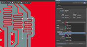
Coupling capacitors find plenty of uses in analog applications and on differential protocols, acting essentially as high pass filters that remove DC bias carried seen on a signal. In the case of PCIe, there are a few reasons to place AC coupling capacitors on differential pairs beyond the fact that AC coupling capacitors are listed in the standard. In this article, we’ll look briefly at where to place coupling capacitors on PCIe links, as well as the reasons these are placed on PCIe links.
Blog
•
Altium Designer 22.7 Update
We are happy to announce that the Altium Designer 22.7 update is now available. Altium Designer 22.7 continues to focus on improving the user experience, as well as performance and stability of the software, based on feedback from our users. Check out the key new features in the What's New section on the left side of this window!

Blog
•
The Positive Impact of Supply Chain Visibility on Design to Cost
Design to cost is a lofty idea that is only perfectly executed when supply and demand for components are in perfect harmony. Unfortunately, the current landscape for component sourcing makes design to cost more of a balancing act rather than an exercise in price reduction. To help designers in their efforts to balance cost, capabilities, and procurement, we created this ebook to help users understand how modern supply chain tools can help in these complex design problems.

Blog
•
A Brief Study of Stubs on a PCIe Connector
Stubs are an important topic in high-speed PCB design, and there is a longstanding guideline that stubs should always be removed from all vias on high-speed digital interconnects. While stubs are bad for high-speed lines, they do not always need to be removed. What is more important is to predict the loss profile and frequencies, and to floorplan appropriately to try and prevent such losses.

Blog
•
PCB Layout Cleanup Before Manufacturing
Once you finish your placement and routing in your PCB layout, it can be tempting to wrap up the layout and send everything in directly to manufacturing. The reality is that the board may still need some work before it is considered finished. The cleanup you perform at the final stage of PCB layout will help you catch any outstanding errors that can't be programmed into your DRC engine, and it gives you a chance to add any outstanding details to the surface layers.

Blog
•
Insulated Metal Substrates: Building an LED Panel
In this project we’ll be building a moderate sized LED panel on insulated metal substrate (IMS). This light panel has three different white balance High CRI LED types on it, warm, neutral and cool. By changing the brightness of the different white balances, the light from the panel can be adjusted to match other lighting, making it perfect for film use - but also creating perfect lighting for electronics work. As with all my projects, this LED panel is open source, you can find the Altium project files over on my GitHub released under the permissive MIT License.

Blog
•
DFM in PCB Material Selection
Every design should begin with selecting the materials that will appear in the PCB stackup, as well as arranging layers in the stackup to support layout and routing. This section of our PCB manufacturing andc DFM crash course focuses on selecting the right materials for your PCB design. Materials should be selected given the particular design requirements outlined in your specifications.

Blog
•
How to Start an FPGA PCB Layout For Your Embedded System
FPGAs come in quad or BGA packages that can be difficult to floorplan, especially with the high number of I/Os often implemented in these components. FPGAs offer a lot of advantages in terms of their reconfigurability, but they can require a lot of effort to layout and route without headaches. If you’ve never worked with an FPGA in your PCB layout, we have some guidelines that can help you get started.

Blog
•
How to Get 3-port S-parameters From a 2-port VNA Measurement
S-parameters are fundamental quantities in signal integrity, and an ability to understand them from measurement or analysis is very important. If you have a 3-port network, like a power divider or circulator, it may appear that you must use a 3-port VNA to measure these S-parameters. It is always acceptable to measure between two ports, but you need to know what exactly it is you are measuring. In this article, we’ll look at the relationship between the true 3-port S-parameters with a 2-port measurement.

Blog
•
A Day in the Life of the PCB Manufacturing Process
Before implementing design for manufacturing, it is important to understand the underlying process behind producing a physical PCB. Regardless of the various technologies present in each facility, a large majority of industry-leading manufacturers follow a specific set of steps to turn your design from a drawing in a CAD application into a physical board. In this article, we'll cover the basics that designers need to know as part of our crash course series on PCB manufacturing.

Blog
•
Addressing Skew Sources in High Speed PCBs
If you compile a list of skew sources, you'll see that fiber weave-induced skew is only one entry on a long list of skew sources. We'll look at this list of possible skew sources below, and we'll see how they affect the operation of your PCB. From the list below, we'll see that some of these issues with skew are not simply solved by paying attention to the fiber weave construction in a PCB substrate.

Blog
•
Should Ground Be Placed Below Inductors in Switching Regulators?
We love answering questions from our readers and YouTube viewers, and one of the recent questions we received relates to EMI from switching elements in a switching regulator is "Should a cutout be placed below the inductor in a switching regulator circuit?". Despite the variations in inductors and their magnetic behavior, there are some general principles that can be used to judge the effects of placing ground near inductors in switching regulator circuits. We’ll look at some of these principles in this article

Blog
•
Altium Designer 22.6 Update
We are happy to announce that the Altium Designer 22.6 update is now available. Altium Designer 22.6 continues to focus on improving the user experience, as well as performance and stability of the software, based on feedback from our users. Check out the key new features in the What's New section on the left side of this window!

Blog
•
Join PCB Design Review Competition from Altium
Find 9 mistakes in a PCB design and get added into the lucky draw to win a prize from Altium!

Blog
•
SAP (Semi-Additive PCB Process) – Top 5 Questions Regarding Stack Up
This Semi-Additive Process is an additional tool in the PCB fabricators' toolbox that enables them to provide feature sizes for trace width and spacing that are 25 microns, (1 mil) and below depending on the fabricators' imaging equipment. This provides much more flexibility to breakout out tight BGA areas and the ability to shrink overall circuit size and/ or reduce the number of circuit layers in the design. As the PCB design community embraces the benefits of this new printed circuit board fabrication technique, there are of course many questions to be answered.

Blog
•
Improving Supply Chain Success with BOM Management
It’s no secret that component shortages have become more frequent this year. In fact, countries around the world are losing billions in revenue due to supply issues. Having the right components on hand is more crucial than ever as availability, obsolescence, counterfeit products and environmental non-compliance risks continue to grow. Fortunately, many shortages can be avoided by introducing proactive supply chain practices.


Your search returns no results.


