Welcome, Guest

Sign in to learn, create, and do more with the product you love.

News & Updates

Filters:
Tag
Embedded thumbnail for PCB Classes overview
How-To's
PCB Classes overview

Are there too many primitives on the board? Having trouble creating design rules? This video gives a brief overview of the classes of primitives that can be created on the board, as well as the possibilities for their further use.

Blog
Ebook: Routing High-Density Interconnects with Reliable Microvias

HDI PCBs take a particular approach to routing interconnects through multiple layers to ensure reliability during fabrication, assembly, and operation. The critical structure that enables this is microvias, which are prone to failure if not designed properly. In this e-book, readers will receive an initial look at the reasons microvia reliability has come into the spotlight and why HDI PCB designers put reliability first when routing through microvias.


Embedded thumbnail for Creating a BGA Footprint with the Footprint Wizard
How-To's
Creating a BGA Footprint with the Footprint Wizard

Altium Designer makes it easy to create a BGA footprint using our IPC compliant footprint wizard. We'll show you how easily you can create and modify a BGA footprint using the footprint wizard.

Blog
IPC-2221 Calculator for PCB Trace Current and Heating

Aside from impedance and annular ring calculations, one of the other major formulas specified in the IPC 2221 standard relates temperature rise, trace width, and trace current. THere is also the IPC-2152 standard, both include this guidance on designing for thermal reliability, but which standard should we use?

Embedded thumbnail for How to work with Pad Classes on PCB?
How-To's
How to work with Pad Classes on PCB?

Sometimes it is required to set different design rules for a different set of pads on the board. The easiest way is to use pad classes and in this video we'll show you how easy it is to create and apply them.

Embedded thumbnail for How to work with multivariate calculations?
How-To's
How to work with multivariate calculations?

Additional modes for obtaining temperature, parametric dependencies and probabilistic distribution by the Monte Carlo method are performed together with basic calculations and allow expanding the possibilities for analyzing design results.

Embedded thumbnail for How to calculate Transient Analysis?
How-To's
How to calculate Transient Analysis?

Transient Analysis simulates the reaction of a circuit over a period of time. It can be supplemented by Fourier Analysis and the use of Initial Conditions.

Embedded thumbnail for BOM Comments
How-To's
BOM Comments

Convenient interaction and coordination of the Active BOM with the help of comments is possible both from the web version of the project and from the Altium Designer between participants of the same and different roles.

Blog
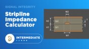
Stripline Impedance Calculator

Striplines provide some advantages over microstrips as they take advantage of natural shielding and coupling from nearby ground plane layers. Although they tend to experience higher losses due to total confinement in the dielectric, they can be thinner due to the high dielectric constant used in internal layers of a PCB. Use our free impedence calculator to help you determine the correct width needed to hit a target impedance.

Embedded thumbnail for Query Language: What is It For?
How-To's
Query Language: What is It For?

A PCB project contains many different objects. How to manage them? How to find the right ones quickly and efficiently? This video starts the series about query language. Learn the language commands and how to use them and expand your possibilities!

Blog
Which Types of Opto-Isolators Are Right For Your Signal?

An optoisolator is a cool electronic device that can be used to pass information between a diode without passing an electrical current. There are many great applications for these, but do you know which one is right for you?
Blog
Properties panel document options in SCH editors

The Properties panel provides access to the properties of documents and objects. The contents of the panel change depending on the active document or the selected object. This blog will quickly go over some of need to know options around the properties panel in the schematic document.

Embedded thumbnail for PCB design with BGA: Via-in-Pad
How-To's
PCB design with BGA: Via-in-Pad

We’ll teach you how to use Via-in-pad to reduce inductance, improve signal integrity, and improve power distribution system performance.

Embedded thumbnail for Design RF PCB: Distributed-Element Circuits
How-To's
Design RF PCB: Distributed-Element Circuits

Distributed-element circuits are a topology of a particular shape and size. Filters, power dividers, directional couplers can be built from them. Being calculated in third-party CAD, the topology of such elements can be easily imported into Altium Designer, and we will show you how to do it!

Embedded thumbnail for How to work with components on a rigid-flex board in MCAD
How-To's
How to work with components on a rigid-flex board in MCAD

With MCAD Codesigner you can quickly add and move components from your MCAD tool and update the design automatically in Altium Designer. We’ll show you how to. Add a new component, move components, and change a component’s region in MCAD, and update it to your design in Altium Designer.

Embedded thumbnail for LSM: Impedance profile
How-To's
LSM: Impedance profile

Creating Impedance profiles for transmission lines and how to apply them to the board

High-Speed PCB Stackup Design
Blog
The High-Speed PCB Stackup Design Challenge

Even with all the good guidelines out there for high speed design, there are particular aspects of stackup construction and their relation to building boards that get overlooked. This blog is goes beyond just the typical SI/PI guidelines and looks at these problems from more of an engineering perspective.

Embedded thumbnail for Multichannel Schematic: Creating Channels
How-To's
Multichannel Schematic: Creating Channels

Altium Designer makes creating single and multichannel designs effective and quick. We’ll show you how to create and annotate output and input channels in your design.

Embedded thumbnail for How to efficiently use Blankets?
How-To's
How to efficiently use Blankets?

Blanket is a powerful tool for group assignment of properties in schematic documents. It makes it easier and faster to assign circuit classes, differential pairs, and design rules within schematic documents. This video provides instructions on how to use blanket to simplify work in your designs.

stitching vias
Blog
Everything You Need to Know About Stitching Vias

Stitching vias are something you often see spread around the surface layer of a PCB, but what are they? and should you be using them? In this guide, we'll go over some of the standard uses of stitching vias and when they should be used in a PCB.

Tag
Rigid-Flex Applications
Blog
Flex and Rigid-Flex PCB Applications

There are two basic reasons for designing a flex circuit into your product: to build a compact and efficiently assembled device, or to make the circuit dynamically integrated with the mechanical function of the product. You may, of course, lean on both of these reasons for justifying the use of flex circuits. On this note, let’s look at some rigid-flex PCB applications and design examples to see the issues that spring to mind when designing flex circuits

Sharing Settings in Altium 365
Blog
Granular Sharing — Role and Group Management

With Altium 365, you can grant permission to teams or users based on the specific needs of a project. We have expanded Altium 365’s file-sharing setting, giving you more granular control over who can download source files and reshare projects with others

Use your DRCs
Blog
Design Rule Checking in the PCB Design Workflow

Any time you design a PCB, and you want to turn it into a real product, you will have to make sure the design obeys the constraints within the standard PCB manufacturing process. This imposes multiple rules on any design, and ECAD software will enforce design rules as you create the board to ensure you obey these important constraints. Make sure you enforce the right design rules at the beginning of the PCB design workflow 

How to select high frequency materials
Blog
Best Practices for High-Frequency PCB Material Selection

High frequency PCB design can seem esoteric, and I've heard many an engineer describe it as "black magic"! The subject is also a bit confusing, especially once someone asks which frequencies could be reasonably considered "high". Before you do anything inside the layout for a high-speed or RF PCB, you will need to pay attention to the materials being used in the board. If you're unsure which high frequency PCB materials you should use, then keep reading to learn more.

PCB Noise Reduction
Blog
PCB Noise Reduction: Do You Need Isolation, Shielding, or Filters?

Of all the noise and operational challenges designers face in their PCBs, there is one overarching problem that is arguably most popular: electronic noise. It could originate as an SI/PI problem, it could possibly arise from some external source, or it could be good old-fashioned crosstalk! These tend to fall into three categories: adding shielding, doing something to create isolation, or placing filters. Let's look at all of these as they tend to be the default solution set when confronted with many noise problems.

What’s New in Altium 365
Blog
What’s New in Altium 365: Version Control for Hardware, Layer Stackup in Web Viewer, and SOC 2 Type 1 Certification

In February, we hit a new record in the number of users on the platform. The Altium 365 user community is now 20,000 strong! You can now migrate from an external version control system to Altium 365 preserving the history of commits. We also received the SOC 2 Type 1 certification from KPMG, made layer stack available in the web viewer, and added the brand new capability to track tasks in the context of your design project. Keep reading to learn more!

Rigid-Flex in Altium Designer
Blog
Support for Rigid-Flex in Altium Designer

Rigid-flex in Altium Designer starts with designing a manufacturable PCB layer stack complete with via transitions and any calculated impedance requirements. Flex sections also need to be placed in the layer stack before moving into the PCB layout. Once inside the PCB editor, bending lines can be clearly defined in the PCB layout, and these can be visualized in Altium Designer's 3D PCB design tools. Keep reading to see how Altium Designer supports your flex and rigid-flex designs.

Specifying your stackup
Blog
Communicating PCB Layer Stackup Needs to Manufacturers

In the business of PCB design, communicating needs to manufacturers and vendors is a top priority. The context of our requests is sometimes lost either by not providing the correct information, not listing enough information, or not giving any information. Although the experienced PCB designer can take steps to specify everything they want to see in their PCB stackup, eventaully the manufacturer will handle that decision in an effort to balance available materials with processing capabilities and yield.

Risk Vs. Reward
Blog
Risk Vs. Reward

During the recent IPC APEX expo, there was a lot of discussion about SAP, or semi-additive PCB processes.  As with any new technology adoption there were people that are excited to jump right in and start designing with much finer feature sizes and work through the inevitable changes to the traditional thought process. Others are in a "let’s wait and see" mode and of course there are a few skeptics there as well, so keep reading to learn more.

Parasitic Extraction for your traces
Blog
Parasitic Extraction with an Electromagnetic Solver in PCB Routing

Parasitic extraction: the integrated circuit design community must grapple with this task on a daily basis, especially once gate features are reduced below ~350 nm and chips run at high switching speeds. The PCB community also has to deal with this idea in order to better design power delivery networks, interconnects with precise impedance, and properly quantify crosstalk and coupling mechanisms.

PCB
Blog
Ebook: PDN Simulation and Analysis Guide

Most designers don’t realize they need to worry about power integrity until they have a power integrity problem. Other designers might build boards that can’t handle the demands of modern digital and high frequency components, and they may not realize the problems that lurk in their power delivery network (PDN). Although the basic concepts involved in designing for power integrity are well-known, myths about power integrity abound, and designers need tools to help them evaluate and qualify power integrity in a PDN.

Ferrites in PDN Simulation
Blog
Ferrite Beads and Transfer Impedance in a PDN Simulation

The use of ferrites in a PDN is one design recommendation that is fraught with unclear guidance and over-generalized recommendations. If you see an application note or a reference design that recommends placing a ferrite in a PDN, should you follow this in your specific design, or should you ignore this and focus on adding capacitance? 

PCB Design Outputs
Blog
Overview of PCB Design Output Files

Before your board can be put into production and prepared for assembly, you have to generate a set of files that assist your manufacturer. These are your PCB design output files, also known as manufacturing files, fabrication data, assembly files, and a host of other names. Before you send your design file off to a manufacturer in an email, make sure to get a list of their required fabrication and assembly files first. If you’re a new designer, take some time to read over the basic PCB manufacturing file extensions below.

How transformers work
Blog
Transformer Theory Made Simple

Transformers can provide very effective signal isolation and are used to manipulate AC voltage and current levels. They can achieve all this with a greater than 95% power efficiency, which is why we commonly see them used in bench power supplies, audio gear, computers, kitchen appliances, and wall-warts. However, transformer theory can be unintuitive and in this article we answer on questions about them

Take advantage of the VCS-based workflow in Altium 365
Blog
Using Altium 365 Over Your Vanilla Version Control System

There are all sorts of version control systems (VCS) out there that people have been using with their PCB design software. As discussed in Why Use a Version Control System, we looked at different options ranging for local hard drive storage to sophisticated online revisioning systems. In this article we will be reviewing the differences between a standard VCS and Altium 365.

Tag
Embedded thumbnail for AI PCB Layout vs. Human Design: The Honest Truth
How-To's
AI PCB Layout vs. Human Design: The Honest Truth

The question is: Can AI really route a PCB as well as an experienced human designer? In this video, we set out to find the answer. Our expert, Zach Peterson, puts it to the test in a side-by-side layout review. The challenge is based on a LinkedIn post where viewers had to guess which board was AI-generated and which was designed by a human.

Embedded thumbnail for Improve Your 3D Wire Bonding Workflow
New in Altium's Software
Improve Your 3D Wire Bonding Workflow

Check out the video where we showcase enhanced wire bonding features, including precise bond wire shape definition, improved clearance checking, streamlined import and export workflows, and efficient management of wire bonding objects.

Embedded thumbnail for Customize Your ODB++ Output for Each Partner
New in Altium's Software
Customize Your ODB++ Output for Each Partner

You can now precisely control what design data is included in your ODB++ outputs for different manufacturing recipients. Choose which signal layers to export, decide how the netlist is handled (included, disabled, or neutralized), and control whether component data is removed or shared without properties.

Embedded thumbnail for Proper Voltage Built a Universal Battery Platform with Altium
Altium Stories
Proper Voltage Built a Universal Battery Platform with Altium

Watch our latest customer success story to see how Proper Voltage partnered with Altium to accelerate high-power battery development for next-generation robotics. With our software, they streamlined collaboration, sped up design reviews, improved sourcing visibility, and reduced risk.

Embedded thumbnail for Improve Readability with Custom Pin Spacing
New in Altium's Software
Improve Readability with Custom Pin Spacing

You can now control the vertical spacing of a pin’s designator and name with a custom margin. This setting can be applied globally via Schematic Preferences or adjusted individually in the Pin properties.

Embedded thumbnail for Does Decoupling Capacitor Placement Actually Matter?
How-To's
Does Decoupling Capacitor Placement Actually Matter?

Our new video tackles common questions about capacitor placement on a PCB. Expert Zach Peterson explains why placement is often less critical on multilayer boards with well-designed power and ground planes and shares the key insights most application notes leave out.

Embedded thumbnail for Teaching Power to Think - How Proper Voltage Accelerates Innovation with Altium
Altium Stories
Teaching Power to Think - How Proper Voltage Accelerates Innovation with Altium

Watch the video where you can find how Proper Voltage centralized communication, synchronized ECAD–MCAD development, and gained early insight into supply chain risks using Altium’s connected design platform.

Embedded thumbnail for  Detect Z-Axis Clearance Issues Earlier
New in Altium's Software
Detect Z-Axis Clearance Issues Earlier

The Z-axis clearance rule enables accurate verification of minimum interlayer copper spacing. It supports targeted constraints between net classes, differential pairs, and schematic parameter directives for advanced rule definition.

Embedded thumbnail for Fix Inconsistent Part Parameters in Your PCB Schematic
How-To's
Fix Inconsistent Part Parameters in Your PCB Schematic

Watch our latest video to learn what parameterization really means, why getting the manufacturer name and part number right is essential, and how to quickly identify inconsistencies across your schematic components using Altium’s Parameter Manager tool.

Embedded thumbnail for Create IPC-Aligned Footprints with Less Effort
New in Altium's Software
Create IPC-Aligned Footprints with Less Effort

The default value for the Solder Mask Expansion rule has been updated to improve consistency across design environments. In both PCB documents and rule-driven solder mask expansion within PCB library documents, the default setting is now 0 mil, replacing the previous default of 4 mil.

Embedded thumbnail for Via Dispersion: Why Propagation Delay Changes with Frequency
How-To's
Via Dispersion: Why Propagation Delay Changes with Frequency

Explore the concept of via dispersion and how it impacts propagation delay across frequencies. This tutorial walks through the math behind extracting delay from insertion loss and return loss S-parameters and explains why results can vary depending on your operating range.

Embedded thumbnail for Make Via Rule Configuration More Intuitive
New in Altium's Software
Make Via Rule Configuration More Intuitive

Set precise control over your routing via styles with new rule settings in the Physical View. Define minimum, maximum, and preferred values for both diameter and hole size, and easily switch between constraint ranges or template-based definitions for faster, more flexible design.

Embedded thumbnail for Coplanar Ground Done Right: PCB Design Best Practices
How-To's
Coplanar Ground Done Right: PCB Design Best Practices

When is coplanar ground actually useful and when does it provide no benefit at all? If you’ve ever wondered about this, check out our brand-new video where we tackle one of the most common questions in PCB design.

Embedded thumbnail for Import and Export with Modern Mechanical Models
New in Altium's Software
Import and Export with Modern Mechanical Models

We have expanded mechanical integration by adding support for SOLIDWORKS 2024 and SOLIDWORKS 2025 part models when importing 3D bodies into the design environment. This enhancement allows designers to work with the latest mechanical models created in SOLIDWORKS without the need for additional conversions or workarounds.

Embedded thumbnail for How to Input Via Delay in Altium for DDR Routing
How-To's
How to Input Via Delay in Altium for DDR Routing

In this video, we tackle a real viewer question about DDR3 routing across multiple PCB layers and show how via delay can silently eat into your skew margin before you’ve even finished routing, using Altium’s default 10-layer stackup as a reference.

Embedded thumbnail for Clearly Show Jumper Wires in Your Harness Designs
New in Altium's Software
Clearly Show Jumper Wires in Your Harness Designs

Support has been improved so that jumper wires connecting two cavities within the same connector are now properly shown in Layout Drawings, making the connector wiring easier to understand during documentation and review.

Tag
Your search returns no results.